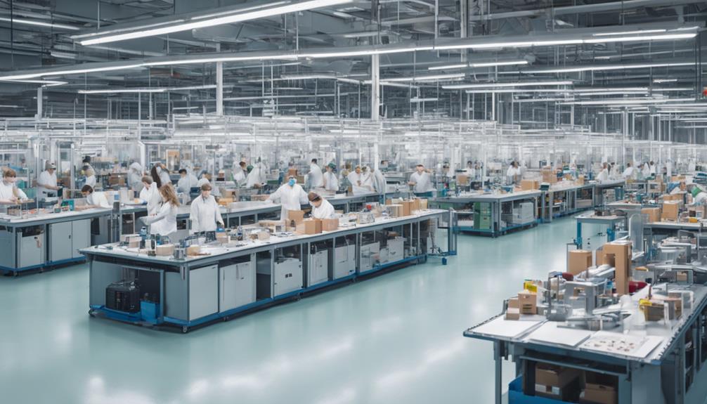
The assembly of electronic boards involves a meticulous sequence of processes, from pre-assembly preparation to final inspection and testing, requiring precision, control, and attention to detail to guarantee the production of reliable and functional electronic devices. The process begins with pre-assembly preparation, involving component organization and PCB inspection, followed by solder paste printing, component placement, and reflow soldering. Through-hole component insertion, wave soldering, and final inspection and testing are also critical stages. By understanding each step, manufacturers can secure the quality and reliability of their electronic boards, and discover the nuances of the assembly process that ultimately lead to superior products.
Key Takeaways
- Pre-assembly preparation involves gathering components, inspecting PCBs, and preparing soldering equipment to ensure a smooth assembly process.
- Solder paste printing quality is influenced by techniques, stencil design, and paste viscosity, with ideal viscosity ranging from 300,000-400,000 cP.
- Component placement requires precision and accuracy, with automated pick-and-place machines achieving high-speed and precise placement.
- Reflow soldering melts solder paste to form strong bonds between components and PCB, with controlled heating profiles ensuring reliability and functionality.
- Final inspection and testing involve visual examination, ICT testing, X-ray inspection, and post-reflow AOI to detect defects and ensure quality standards.
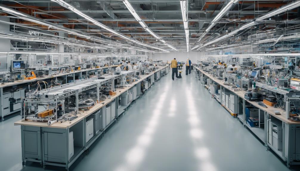
PCB Assembly Line Process Flow
The PCB assembly line process flow begins with the application of solder paste stenciling, a crucial preparatory step for component placement. This pivotal stage guarantees accurate and efficient assembly of components onto the PCB. The solder paste, carefully applied through a stencil, provides a strong bond between the components and the PCB.
The assembly process then continues with the placement of components using Surface Mount Technology (SMT) and Thru-Hole Technology (THT). SMT involves the automatic placement of small components, while THT requires manual insertion of larger components.
After component placement, the PCB undergoes reflow soldering, where the components are heated to securely bond them to the PCB.
To uphold the integrity and functionality of the assembled PCB, optical inspection and quality control checks are carried out. These essential stages confirm the correct placement and soldering of components, ensuring the reliability of the final product.
PCB Design and Manufacturing
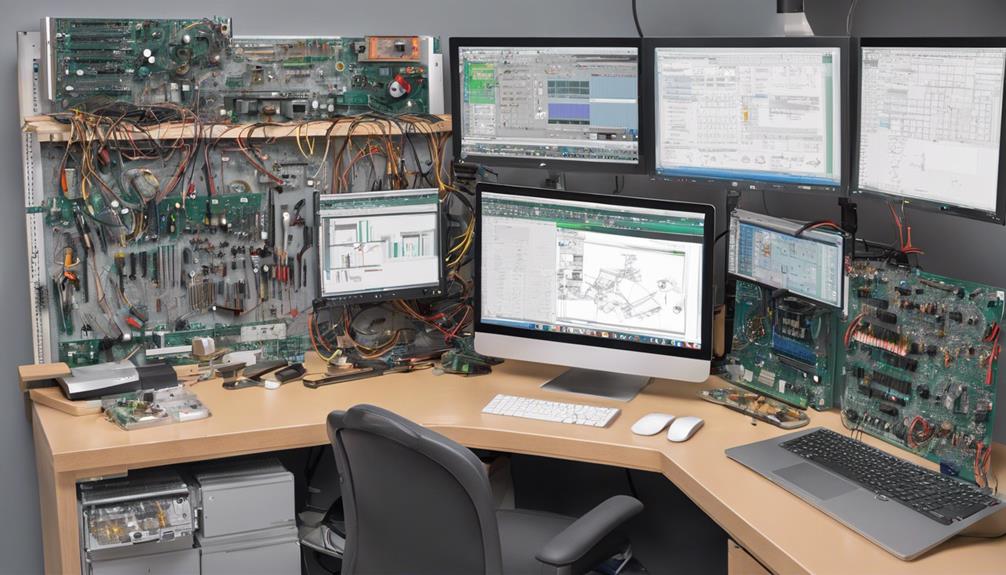
When undertaking PCB design and manufacturing, it is crucial to prioritize prototyping essentials and design for manufacturability (DFM) principles.
By doing so, designers can guarantee that their board designs are optimized for seamless fabrication, reducing the risk of defects and production delays.
PCB Prototyping Essentials
PCB prototyping, an essential step in electronic board assembly, involves designing the circuit layout and creating the initial board design to test functionality and identify potential flaws. This critical phase enables the detection of design flaws, optimization of the PCB layout, and verification of the board's functionality.
| Prototyping Phase | Key Activities |
|---|---|
| Circuit Design | Designing the circuit layout and creating the initial board design |
| Component Placement | Placing components such as resistors, capacitors, and ICs on the prototype board |
| Testing and Optimization | Testing functionality, identifying design flaws, and optimizing the PCB layout |
Gerber files, containing information on layers, components, and copper traces, are essential for PCB manufacturing. Efficient prototyping streamlines the PCB assembly process, leading to successful production runs. By following a structured prototyping process, engineers can guarantee that their designs are reliable, efficient, and cost-effective.
Design for Manufacturability
Optimizing electronic board assembly through efficient prototyping paves the way for design for manufacturability, an essential aspect of PCB design that considers various factors to guarantee seamless production. Design for Manufacturability (DFM) is a critical step in ensuring that PCB designs are optimized for assembly, minimizing errors and production costs.
A thorough DFM check is important to identify potential issues, such as component clearance, solder mask alignment, and copper trace width, which can hinder manufacturability. To facilitate this process, design files containing Gerber, BOM, and assembly drawings are necessary.
Collaboration between design engineers and manufacturing teams is crucial to address DFM issues early in the design phase, streamlining the PCB assembly process. By optimizing PCB designs for manufacturability, manufacturers can reduce production costs, minimize assembly errors, and accelerate time-to-market for electronic products.
Effective DFM checks and collaboration ensure that manufacturing constraints are considered, resulting in high-quality PCBs that meet specifications and performance requirements.
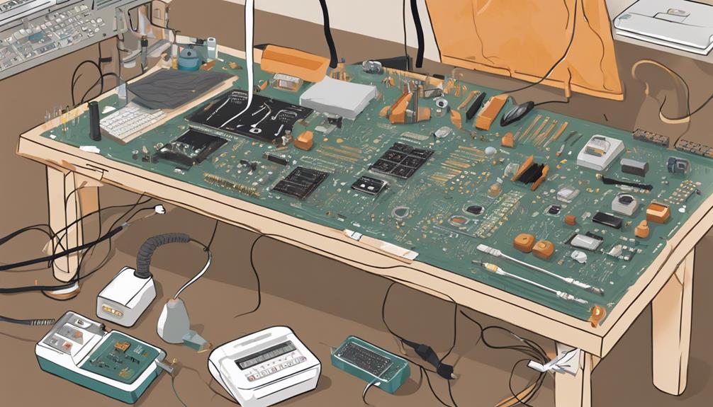
Pre-Assembly Preparation Steps
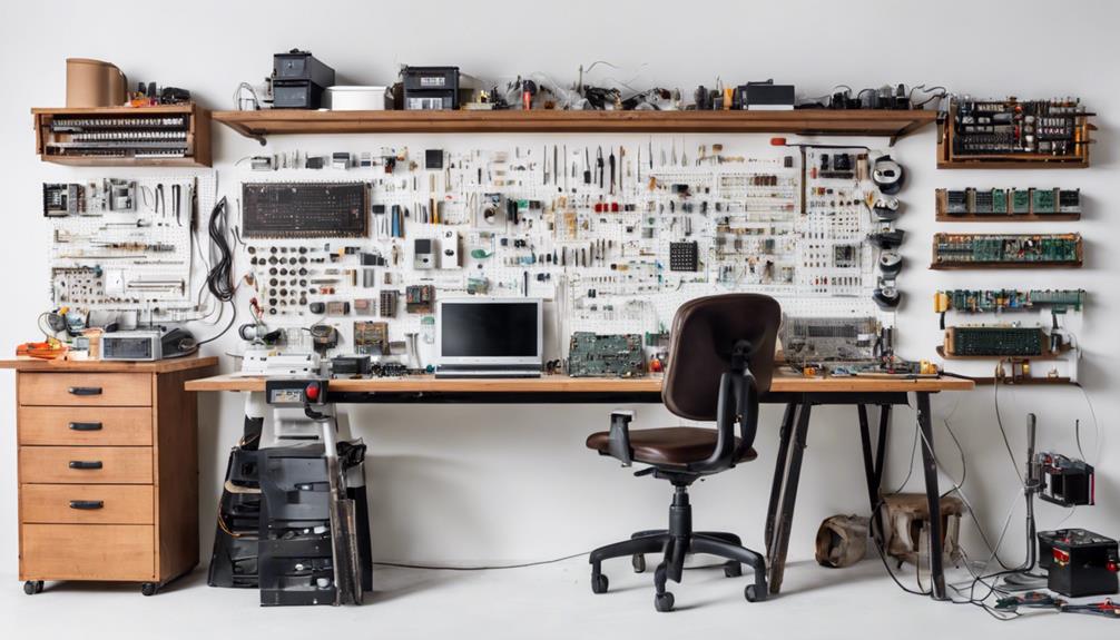
Gathering all necessary components, tools, and materials in a clean and organized workspace is crucial to guaranteeing a successful electronic board assembly process. At a reputable PCB assembly company, pre-assembly preparation is a critical step that sets the stage for a high-quality assembly process.
This involves organizing components according to the Bill of Materials (BOM) to ensure accuracy during assembly. PCBs are also inspected for defects or damage before the assembly process begins, ensuring that only defect-free boards are used. Soldering equipment, such as soldering irons, flux, and solder wire, are checked and prepared for use.
Additionally, proper ESD protection measures are implemented to prevent static damage to sensitive electronic components during assembly. A clean workspace is maintained to prevent contamination and ensure the quality of the assembled boards. By following these pre-assembly preparation steps, a PCB assembly company can guarantee a smooth and efficient assembly process that produces high-quality electronic boards.
Solder Paste Printing Process
In the solder paste printing process, the quality of the printed deposit is influenced by various factors. These include the techniques employed, stencil design, and paste viscosity. Understanding the evolution of past printing techniques is crucial to appreciate the advancements in modern solder paste printing.
This section will examine the key considerations in stencil design, ideal paste viscosity, and their impact on the overall printing process.
Past Printing Techniques
Within the domain of surface mount assembly, solder paste printing has emerged as a critical process step. Accurate deposition of solder paste onto PCB pads is paramount for guaranteeing reliable component attachment. The solder paste printing process involves applying solder paste onto PCB pads using a stencil. The stencil design and thickness greatly impact the volume and placement accuracy of solder paste.
Proper alignment and pressure control during printing are essential to guarantee consistent solder paste application. This directly affects component adhesion during assembly. In the past, various printing techniques have been employed to achieve the best solder paste deposition. These techniques have evolved over time, with advancements in stencil design and printing mechanisms enabling improved solder paste volume control and precision.
Stencil Design Considerations
What specific stencil design parameters can be optimized to achieve accurate solder paste deposition and reliable component attachment in surface mount assembly?
Stencil design plays an important role in ensuring accurate solder paste application and component alignment during PCB assembly. The aperture size, shape, and alignment on the stencil have a significant impact on solder paste deposition and overall assembly quality. A well-designed stencil guarantees consistent solder paste volume, which is essential for reliable solder joints.
Proper stencil thickness is essential to achieve this consistency. Moreover, stencil tension and frame rigidity are crucial for maintaining stencil flatness during the printing process. This ensures that the solder paste is applied evenly and accurately.
Additionally, regular stencil cleaning and maintenance are necessary to prevent solder paste bridging and ensure consistent printing results. By optimizing these stencil design parameters, manufacturers can achieve high-quality solder joints and reliable component attachment, resulting in improved overall assembly quality.
Optimal Paste Viscosity
Ideal paste viscosity is a critical factor in the solder paste printing process, as it directly affects the consistency and quality of solder paste deposition, building upon the foundation established by a well-designed stencil.
The ideal viscosity range for effective stencil release and component adhesion is typically between 300,000-400,000 cP. Viscosity plays a key role in paste transfer efficiency, with low viscosity causing solder balling and high viscosity leading to insufficient solder deposition.
Achieving the desired viscosity ensures consistent solder paste deposits, minimizing defects like bridging or insufficient solder joints. Temperature control and rheology modifiers can be employed to adjust viscosity, achieving ideal paste flow during the printing process.
Monitoring and controlling paste viscosity are crucial for achieving high-quality solder paste printing results in PCB assembly. By optimizing viscosity, manufacturers can guarantee reliable component adhesion, precise solder deposition, and reduced defects, ultimately resulting in high-reliability electronic assemblies.
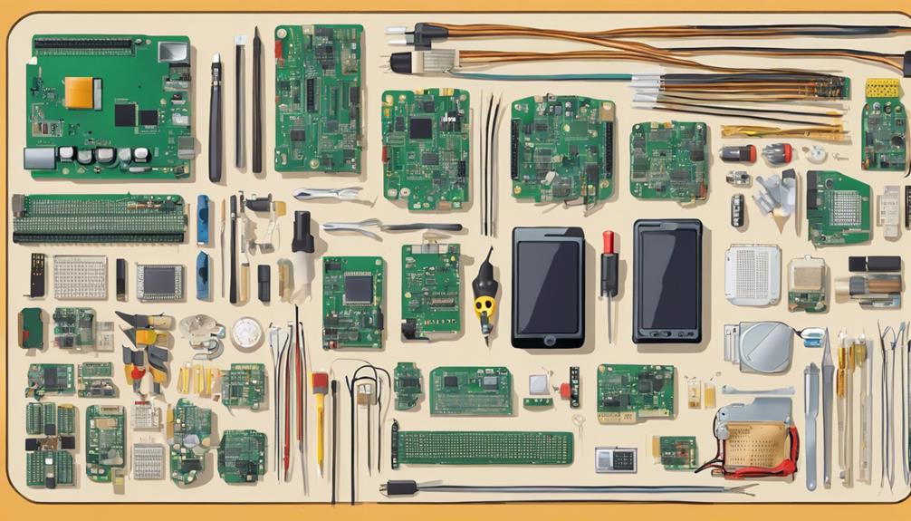
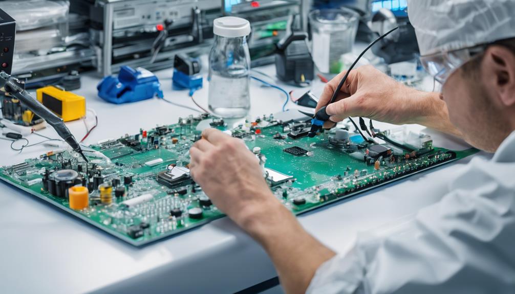
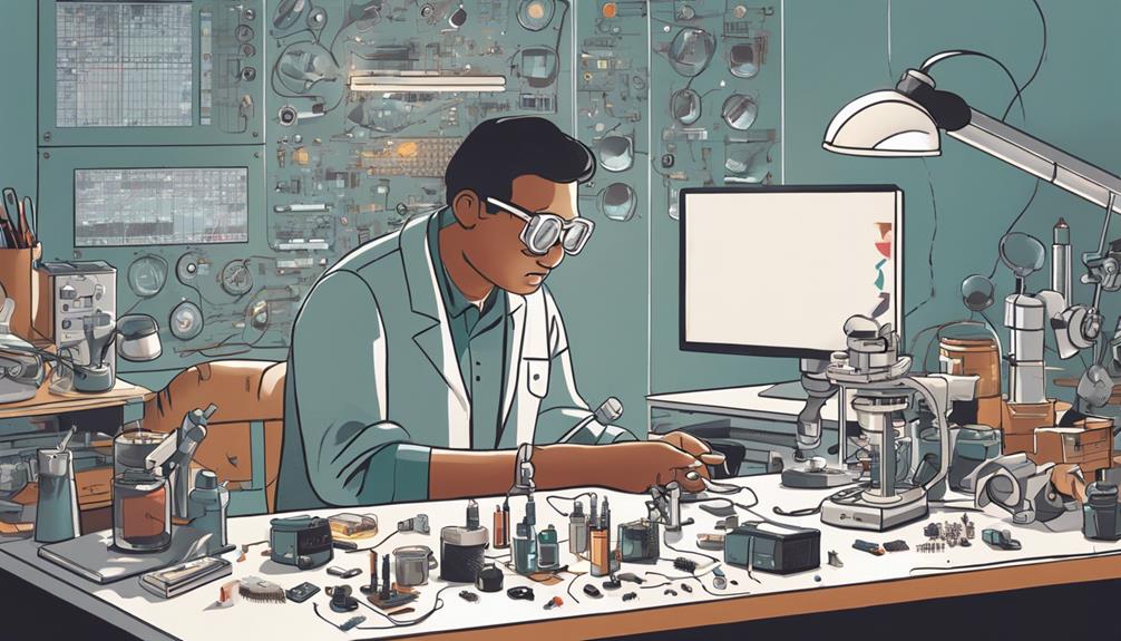
Component Placement and Inspection
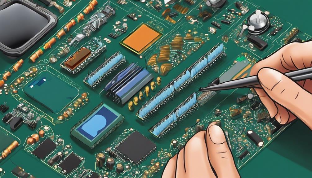
Component placement, a critical stage in the assembly of electronic boards, involves the precise positioning of electronic parts on the printed circuit board (PCB) according to the design layout. This process requires accuracy and precision to guarantee the functionality, reliability, and performance of the electronic board.
Automated pick-and-place machines are often utilized to achieve high-speed and precise component placement. These machines enable the rapid and accurate positioning of electronic parts on the PCB, ensuring that the assembly process is efficient and effective.
Following component placement, a visual inspection is conducted to verify the correct orientation, alignment, and soldering of components. This inspection is vital in identifying any errors or defects early in the assembly process, allowing for prompt corrections to be made.
Inspection after component placement is an essential step in ensuring the quality and reliability of the electronic board. By combining accurate component placement with thorough visual inspection, manufacturers can guarantee that their electronic boards meet the highest standards of quality and performance.
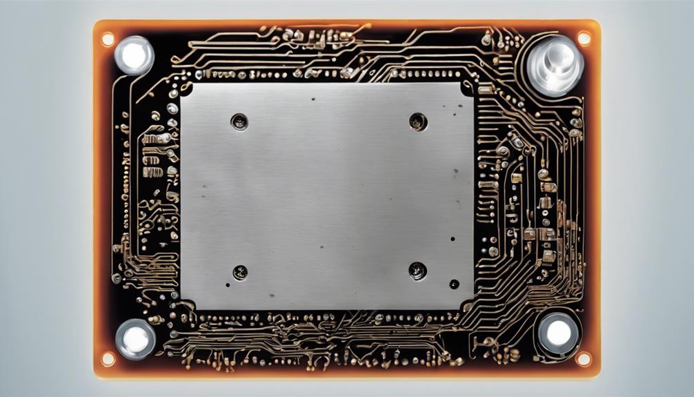
Reflow Soldering and X-Ray
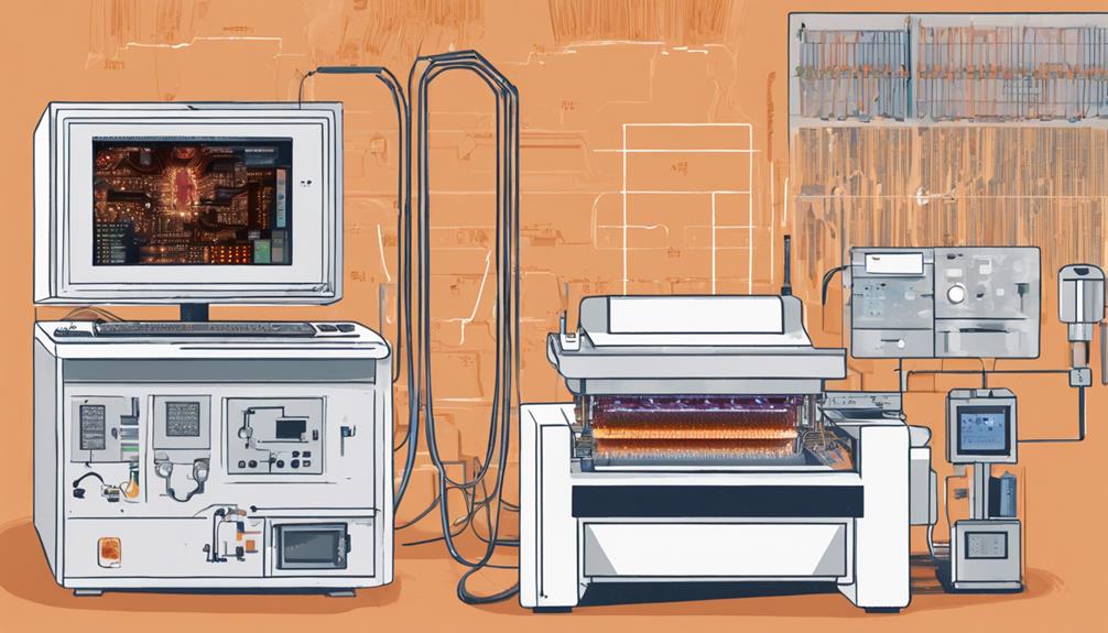
The reflow soldering process is a critical step in assembling electronic boards, where controlled heating profiles are used to melt solder paste and form secure bonds between components and the printed circuit board (PCB).
Meanwhile, X-ray inspection techniques are employed to non-destructively test PCBs, detecting hidden defects and guaranteeing the quality and reliability of the assembly.
Reflow Soldering Process
In the assembly of electronic boards, the reflow soldering process is a vital step where solder paste is melted to form strong bonds between surface-mount technology (SMT) components and the printed circuit board (PCB).
This process involves carefully controlled heating profiles to guarantee proper solder melting and component attachment. The reflow process is essential in securing the reliability and functionality of electronic boards.
Solder paste is applied to the PCB, and then the board is subjected to a controlled temperature profile, melting the solder and forming strong bonds between the SMT components and the PCB. The heating profiles are carefully designed to prevent overheating, which can damage the components or the PCB.
The resulting solder joints are critical to the board's functionality, and any defects can lead to board failure. Therefore, it is vital to make sure that the reflow soldering process is done correctly to achieve reliable and functional electronic boards.
X-Ray Inspection Techniques
Quality assurance in electronic board assembly relies on the meticulous detection of defects, and X-ray inspection techniques have emerged as an essential tool for uncovering hidden flaws in reflow soldering processes.
X-ray inspection is an important testing method that helps detect defects that may compromise the functionality and reliability of the electronic board.
Here are some key benefits of X-ray inspection in PCB assembly:
- Detection of hidden defects: X-ray inspection can identify hidden defects such as voids, misalignment, and solder bridges that may occur during the reflow soldering process.
- Ensuring solder joint integrity: X-ray inspection provides detailed images of internal structures, ensuring solder joint integrity and component alignment post-reflow.
- Component alignment verification: X-ray machines utilize advanced imaging technology to identify defects like insufficient solder, tombstoning, and component misalignment.
- Enhanced quality assurance: X-ray inspection is an important step in ensuring the quality and reliability of electronic boards, detecting defects that may not be visible to the naked eye.
Through-Hole Component Insertion
Precise placement of leads into pre-drilled holes on the printed circuit board (PCB) is the fundamental principle of Through-Hole Component Insertion. This process involves manually placing larger components with leads into pre-drilled holes on the PCB, ensuring secure connections and reliable electronic assemblies. Through-Hole Technology is preferred for components requiring mechanical strength and heat resistance, such as connectors, switches, and larger capacitors.
| Component Type | Insertion Method | Benefits |
|---|---|---|
| Larger Capacitors | Manual Insertion | Durability and Reliability |
| Connectors | Through-Hole Technology | Mechanical Strength |
| Switches | Wave Soldering | Heat Resistance |
| Components with Leads | Through-Hole Component Insertion | Secure Connections |
Through-Hole Component Insertion offers durability and reliability in electronic assemblies, making it an essential step in the PCB assembly process. By using Through-Hole Technology, components are securely attached to the PCB, ensuring reliable connections and minimizing the risk of component failure. With Wave Soldering, components are soldered to the PCB, providing a strong and reliable bond.
Wave Soldering and Inspection
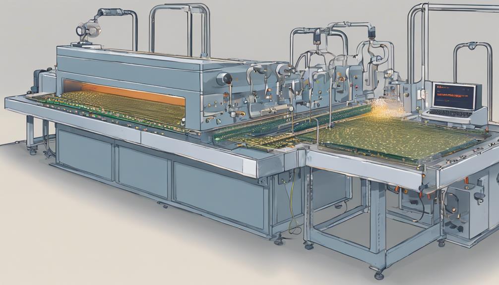
Frequently, the wave soldering process is employed in through-hole technology (THT) assembly to form reliable solder joints on through-hole components, ensuring both mechanical strength and electrical connections. This process involves passing the PCB over a wave of molten solder, which is achieved through a conveyor system that moves PCBs through preheating, fluxing, soldering, and cooling stages.
To guarantee quality, proper wave soldering parameters such as wave height, preheat temperature, and conveyor speed are essential in achieving consistent and reliable solder joints.
The following key factors contribute to successful wave soldering and inspection:
- Optimized wave soldering parameters to prevent defects and ensure reliable solder joints.
- Efficient conveyor systems for efficient production and reduced defects.
- Thorough inspection after wave soldering to detect soldering defects like bridges, insufficient solder, or misaligned components.
- Quality control measures to ensure high-quality PCBs that meet the required standards.
Conformal Coating and Cleaning
In electronic board assembly, conformal coating and cleaning processes play a crucial role in ensuring the reliability and longevity of printed circuit boards (PCBs) by protecting them from environmental stressors and eliminating contaminants that can compromise their performance.
Conformal coatings, such as acrylics, silicones, and urethanes, shield PCBs from humidity, corrosion, and thermal stress, enhancing their reliability. Meanwhile, cleaning processes involving deionized water rinsing remove flux residues, ensuring excellent performance and longevity.
| Coating Type | Properties | Benefits |
|---|---|---|
| Acrylic | Humidity protection | Reliability enhancement |
| Silicone | Thermal stress resistance | Longevity improvement |
| Urethane | Corrosion shielding | Environmental protection |
Proper cleaning and coating procedures are essential for maintaining PCB integrity and functionality in various operating environments. By combining these processes, PCBs can withstand environmental factors, ensuring outstanding performance and longevity.
Final Inspection and Testing
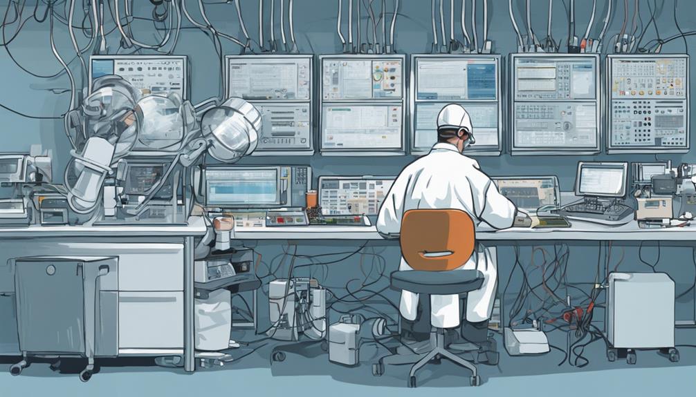
During the final inspection and testing stage, a meticulous evaluation of the assembled printed circuit boards (PCBs) is conducted to verify their compliance with stringent quality standards. This thorough process involves a series of rigorous tests and inspections to make sure the PCBAs meet the required specifications.
The following key steps are taken during final inspection and testing:
- Final Inspection: A visual examination of the PCBAs to detect any defects or anomalies.
- ICT Testing: Automated tests confirm the functionality of electronic connections, guaranteeing reliable performance.
- X-ray Inspection: Detailed examination of components, such as BGAs, to identify defects or irregularities.
- Post-reflow AOI: Automated optical inspection ensures proper component placement and alignment.
Additionally, cleaning and drying the PCBAs thoroughly post-assembly is essential for top performance and longevity.
Packaging and Transportation
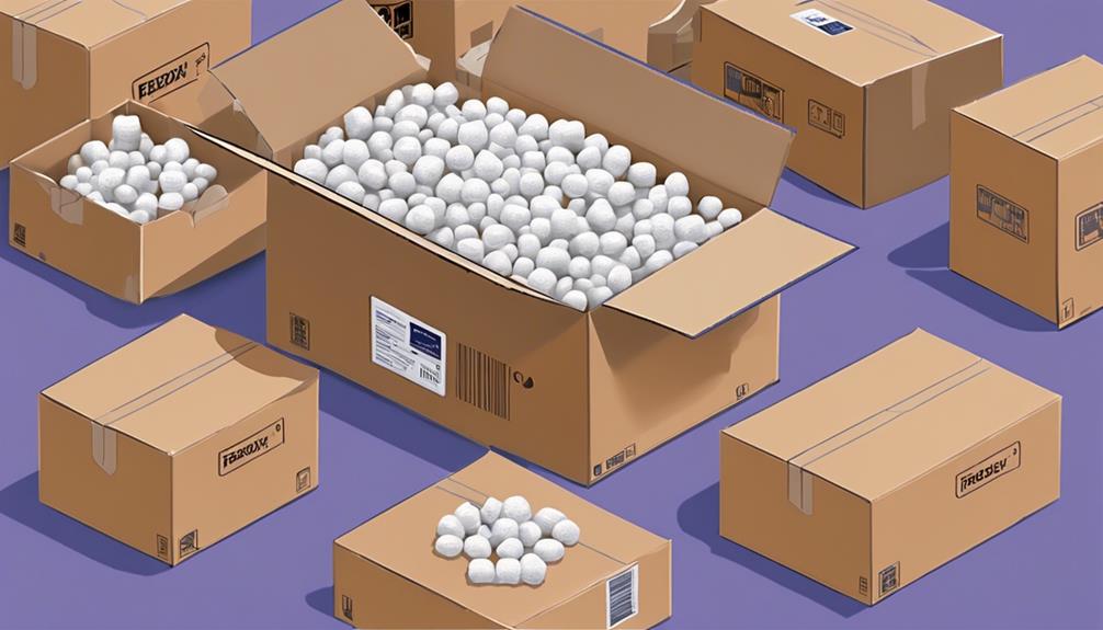
The careful packaging of assembled printed circuit boards (PCBs) is a vital step in the manufacturing process, as it directly impacts the safety and integrity of the electronic boards during transportation.
Proper packaging is essential in safeguarding electronic boards against damage during transit, guaranteeing that they arrive at their destination in pristine condition.
To achieve this, anti-static bags are commonly used to store PCBAs, protecting them from static electricity. Additionally, custom foam inserts provide cushioning and support to prevent impact damage during transit.
For added protection, conformal coating can be applied to shield the boards from environmental factors during shipping.
Careful handling and transport considerations are essential to ensure the safe delivery of electronic boards to customers. This involves meticulous planning and attention to detail to prevent shocks, vibrations, and other forms of stress that could compromise the integrity of the boards.
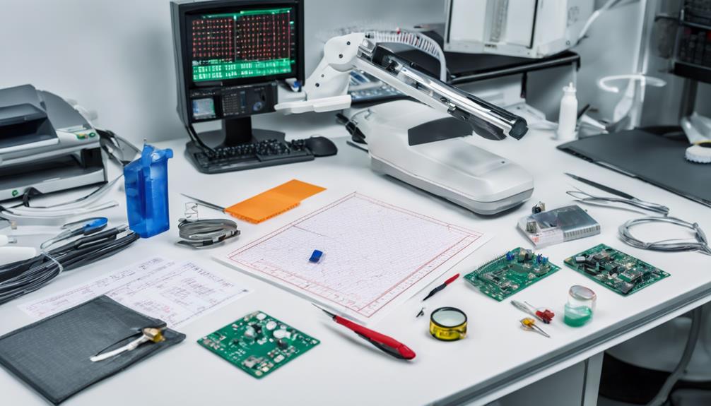
PCB Assembly Quality Control
Upon ensuring the safe transportation of printed circuit boards, attention turns to the meticulous process of quality control in PCB assembly, where precision and attention to detail are paramount. The PCB assembly process involves multiple quality control checks to uphold the highest standards of production.
Key quality control measures include:
- Automated Optical Inspection (AOI): Utilizing advanced optics and software to detect defects and guarantee accurate component placement.
- Manual Soldering Inspection: Technicians visually inspect solder joints for defects, ensuring reliable connections.
- X-ray Inspections: High-resolution X-ray imaging detects defects in complex PCB assemblies, guaranteeing high-quality production.
- Final Inspection and Functional Testing: Verifying the functionality of assembled electronic boards, ensuring they meet specifications.
Throughout the PCB assembly process, quality control is essential. Scrapping failed PCBAs and repeating the assembly process for successful production is crucial for maintaining quality standards.
How Can Visual Process Flow Guide Help Ensure Quality in Electronic Board Assembly?
A visual process flow guide can ensure quality in electronic board assembly by providing a clear, step-by-step overview of the entire process. This includes the checkpoints and quality assurance measures outlined in the comprehensive assembly line checklist. With this visual aid, technicians can easily follow the assembly process, reducing errors and maintaining quality standards.
Finished PCB Handling and Feedback
In the final stages of PCB assembly, meticulous handling and feedback mechanisms are employed to guarantee the integrity of finished printed circuit boards. Finished PCBs are handled with care to avoid damage to components or solder joints during the assembly process.
Each PCB undergoes a final inspection to make sure all components are correctly placed and soldered, and that all connections are secure. This inspection process provides critical feedback, helping to identify any defects or issues that need to be addressed before the PCB is shipped.
Quality control measures are implemented to maintain high standards and meet customer requirements for the finished PCB. Proper handling and feedback mechanisms are vital in delivering reliable and functional PCB assemblies to customers.
Frequently Asked Questions
What Is the Process Flow of PCB Assembly?
The PCB assembly process flow involves a series of sequential steps.
It begins with solder paste application using a stencil to guarantee even distribution on the PCB.
Component placement is then executed using high-precision pick-and-place machines, followed by reflow soldering to bond components to the PCB through controlled heating and cooling cycles.
What Are the 3 Steps in the Circuit Board Assembly Process?
In the vast expanse of electronic manufacturing, a trio of essential steps reign supreme in the circuit board assembly process.
The three indispensable pillars of PCB assembly are solder paste application, component placement, and reflow soldering.
These sequential steps guarantee the seamless integration of electronic components, yielding a functional and reliable circuit board.
What Is the Electronic Assembly Process?
The electronic assembly process involves the precise placement of components, such as resistors, capacitors, and ICs, onto a printed circuit board (PCB). This process utilizes Surface Mount Technology (SMT) or Thru-Hole Technology (THT) methods to mount components, which are then secured using solder paste.
Stringent quality control measures, including optical and X-ray inspections, guarantee accurate component placement and soldering.
What Are the Steps of the SMT Process?
The SMT process unfolds like a precision-crafted orchestral performance, with each step harmoniously building upon the last.
The process begins with the meticulous application of solder paste, carefully distributed onto the PCB using a stencil.
Next, components are precisely placed onto the board via automated pick-and-place machines.
Reflow soldering then melts the paste, bonding components securely to the board.