Seven essential surface mount package types have emerged as important components in modern electronic designs, each offering unique advantages and applications. These include Small Outline Transistor (SOT) Packages, Quad Flat Package (QFP) Variations, Dual Flat No-Lead (DFN) Packages, Ball Grid Array (BGA) Packages, Land Grid Array (LGA) Packages, Small Outline Integrated Circuit (SOIC) Packages, and Chip Scale Package (CSP) Options. Each type is suited for specific applications, such as space-constrained designs, high-power devices, and high-density applications. By understanding the characteristics of each package type, designers can optimize their electronic designs for improved performance and reliability. Further exploration of these package types can reveal more nuanced insights into their capabilities and limitations.
Key Takeaways
- SOT packages offer compact thickness and versatility, supporting various components like power transistors, regulators, and amplifiers.
- QFP variations provide diverse lead counts, pitch sizes, and dimensions, making them suitable for high pin density applications.
- DFN packages excel in compact size and thermal management, making them ideal for space-constrained and high-power applications.
- BGA and LGA packages feature compact footprints and improved thermal and electrical performance, making them suitable for high-density and high-speed signal applications.
- CSP options, such as WLCSP and FOWLP, offer high integration, minimal space requirements, and increased I/O density, making them popular in compact electronic designs.
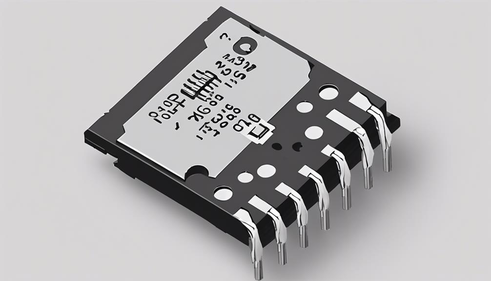
Small Outline Transistor (SOT) Packages
What distinguishes Small Outline Transistor (SOT) packages from other surface mount technologies is their versatility, offering a range of pin counts, lead sizes, and pitches, all within a compact maximum thickness of 1.8mm. This versatility makes SOT packages a popular choice for various applications.
Common SOT package types include SOT-23, SOT-89, SOT-223, SOT-323, and SOT-363, each catering to specific component requirements. For instance, SOT-23 is often used for low-power transistors, while SOT-89 is commonly used for voltage regulators, and SOT-223 for MOSFETs. SOT packages support a wide range of components, including power transistors, regulators, diodes, amplifiers, and optoisolators.
Understanding the characteristics of SOT packages is essential for selecting components that meet specific power requirements and PCB layout constraints. With their compact size and adaptability, SOT packages are an ideal choice for designers seeking to optimize their designs for power and performance.
Quad Flat Package (QFP) Variations
Quad Flat Package (QFP) variations, including Low-profile Quad Flat Package (LQFP) and Thin Quad Flat Package (TQFP), have been developed to cater to diverse design requirements, offering a range of lead counts, pitch sizes, and dimensions that enable efficient circuit layout and space utilization. These variations provide designers with the flexibility to select the most suitable package for their specific application.
- LQFP packages offer reduced heights compared to standard QFPs, enhancing space efficiency and enabling compact designs.
- TQFP packages provide thinner profiles for applications where height constraints are critical, ensuring compatibility with slim devices.
- QFP packages are available with varying lead counts, pitch sizes, and dimensions to accommodate diverse circuit layout needs.
QFP packages are particularly suitable for applications requiring a balance between pin density and space constraints. They provide high pin counts, making them an attractive option for designs that demand a high level of integration. By offering a range of QFP variations, designers can optimize their designs to meet specific performance, power, and space requirements.
Dual Flat No-Lead (DFN) Packages

Dual Flat No-Lead (DFN) packages have emerged as a popular choice for modern electronic designs, offering a unique combination of compact size, excellent thermal management, and improved electrical performance.
These surface mount devices are particularly well-suited for space-constrained applications, where their compact size and low profile enable efficient use of board real estate.
The absence of leads in DFN packages minimizes parasitic effects, resulting in improved high-frequency performance and reliability compared to traditional leaded packages.
Additionally, the exposed pads on the bottom of DFN packages enhance thermal conductivity, allowing for better heat dissipation and thermal management capabilities. This makes them ideal for high-power applications where efficient heat dissipation is critical.
As a result, semiconductor components packaged in DFN packages are increasingly used in a wide range of applications, including high-reliability and high-performance systems.
Ball Grid Array (BGA) Packages

Ball Grid Array (BGA) packages have emerged as a preferred choice for high-density electronic designs, offering a unique combination of compact footprint and robust connections that enable efficient use of board real estate. This is particularly important in IC packaging, where space efficiency is critical.
BGA packages feature contact pads located underneath the package, which are connected using solder balls. The typical ball pitch of 1.27mm ensures reliable soldering.
The advantages of BGA packages include:
- Compact footprint: BGA packages offer reduced footprint compared to other package types, making them ideal for high-density applications.
- Robust connections: The solder balls provide reliable connections, ensuring efficient use of board real estate.
- High pin count: BGA packages can accommodate a high number of pins, making them suitable for complex electronic designs.
When working with BGA packages, it is essential to employ proper PCB assembly techniques to guarantee successful soldering. This is critical in surface mount technology, where small outline packages require precise assembly.
Land Grid Array (LGA) Packages

Land Grid Array (LGA) packages have emerged as a preferred choice for high-performance applications, leveraging an array of lands on the bottom surface to provide reliable electrical connections through solder balls.
Unlike traditional packages with leads, LGA packages feature an array of lands, allowing for improved thermal and electrical performance. This design enables LGA packages to excel in high-performance applications, where high pin counts and compact footprint are essential.
The absence of leads also facilitates better thermal dissipation, making LGA packages ideal for applications where high-speed signals and low inductance are critical. The compact footprint of LGA packages allows for efficient use of board space, making them suitable for applications where real estate is limited.
Small Outline Integrated Circuit (SOIC) Packages
In the domain of Small Outline Integrated Circuit (SOIC) packages, three key aspects warrant examination: package dimensions, pin count options, and thermal resistance.
These factors influence the performance and reliability of SOIC packages, which are widely employed in various IC applications.
Package Dimensions
With their compact footprint and versatility, Small Outline Integrated Circuit (SOIC) packages have become a staple in modern electronics, offering a range of sizes, including SOIC-8, SOIC-14, and SOIC-16, each identified by their corresponding pin count. The standardized package dimensions of SOIC packages guarantee seamless integration with PCB layouts and designs.
The lead pitch of SOIC packages is 1.27mm, facilitating compatibility with various SMD components. The gull-wing leads of SOIC packages enable secure surface mounting, ensuring reliable connections and ease of assembly. The low profile design of SOIC packages makes them ideal for applications where space is limited, making them a popular choice for ICs, amplifiers, voltage regulators, and other integrated circuits.
The package dimensions of SOIC packages are critical in determining their suitability for specific applications. By understanding the package size, pad sizes, and lead pitch, designers and engineers can optimize their PCB designs, guaranteeing efficient use of space and reliable performance.
As a result, SOIC packages have become a cornerstone of modern electronics, powering a wide range of devices and systems.
Pin Count Options
SOIC packages offer a variety of pin count options that cater to different levels of complexity in integrated circuit designs, allowing designers to find a balance between functionality and spatial constraints. The choice of pin count depends on the complexity of the integrated circuit and spatial limitations in the design.
Common pin count options for SOIC packages include 8, 14, 16, 20, and 28 pins, with pin counts typically being multiples of 4 to simplify PCB layout and routing.
The flexibility of SOIC packages regarding pin count enables designers to optimize their designs for specific applications. With a range of pin counts to choose from, designers can pick the most appropriate package for their integrated circuit, ensuring efficient use of space on the PCB.
The equilibrium between pin density and ease of soldering in surface mount technology is a significant advantage of SOIC packages. By offering a variety of pin count options, SOIC packages give designers the freedom to create efficient and effective designs that meet specific performance requirements while minimizing space constraints.
Thermal Resistance
Thermal resistance, a pivotal parameter in surface mount technology, plays an important role in determining the reliability and performance of Small Outline Integrated Circuit (SOIC) packages. In SOIC packages, thermal resistance is typically around 30-70°C/W, indicating their ability to dissipate heat efficiently.
Lower thermal resistance values signify better thermal performance, which is vital for high-power applications. To guarantee optimal performance, it's vital to take thermal resistance into account when designing surface mount packages.
Here are key considerations:
- Thermal resistance impacts the junction-to-ambient thermal resistance and affects the overall operating temperature of SOIC components.
- Proper thermal management techniques like heatsinks or thermal vias can enhance the thermal performance of SOIC packages.
- Understanding thermal resistance values helps in designing effective heat dissipation solutions for SOIC components.
Chip Scale Package (CSP) Options
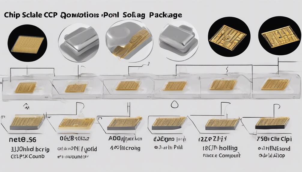
Frequently, chip scale packages (CSPs) are favored in compact electronic designs due to their exceptional ability to integrate complex functionality within a remarkably small footprint.
Measuring less than 1mm on each side, CSPs offer high integration with minimal footprint, making them ideal for space-constrained applications. The elimination of additional packaging components enhances electrical performance, allowing for efficient data transfer and reduced power consumption.
Variants like Wafer-Level Chip Scale Packages (WLCSP) and Fan-Out Wafer-Level Packages (FOWLP) provide advanced features such as increased I/O density and improved thermal management. CSP options include BGA-like designs with solder balls or fan-out configurations, increasing functionality and reliability.
These compact packages are widely used in mobile devices, wearables, and IoT products, where compact size and efficient performance are essential. By leveraging CSPs, designers can create innovative, high-performance devices that meet the demands of modern electronics.
Frequently Asked Questions
What Are the Different Types of SMD Packages?
As the electronics industry continues to miniaturize, the significance of Surface Mount Device (SMD) packages comes to the forefront.
In response to the question, 'What are the different types of SMD packages?', a plethora of options emerge. QFP, BGA, SOIC, and PLCC are popular variants, while LQFP, TQFP, and TSOP cater to specific IC configurations and pin spacings.
Additionally, SOT packages like SOT-23, SOT-89, and SOT-223 are commonly used for discrete components, offering design flexibility and efficiency.
What Are the Different Types of Surface Mount Leads?
Surface mount leads come in various configurations, each with distinct characteristics.
Gull-wing leads, commonly found in SOIC packages, provide mechanical stability during soldering.
J-lead packages, often seen in QFP packages, offer improved thermal and electrical performance.
Flat leads, typically found in PLCC packages, enable low-profile designs for space-constrained applications.
These lead configurations have a substantial impact on soldering processes, thermal management, and overall component reliability in surface mount packages.
What Is the Difference Between SOT and SOIC Package?
The primary difference between SOT (Small Outline Transistor) and SOIC (Small Outline Integrated Circuit) packages lies in their design, application, and characteristics.
SOT packages are smaller, with gull-wing leads, typically used for discrete components like transistors and diodes.
In contrast, SOIC packages are larger, with J-leads, commonly used for integrated circuits.
What Are Surface Mount Packages?
In the domain of modern electronics, a vital question emerges: what are surface mount packages?
The answer lies at the intersection of innovation and efficiency. Surface mount packages are designed for direct placement on printed circuit boards, eliminating the need for drilling holes.
This revolutionary approach enables space-saving designs, improved electrical performance, and streamlined assembly processes. By leveraging surface mount technology, manufacturers can achieve higher component density, faster production speeds, and unparalleled reliability.