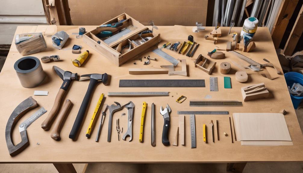
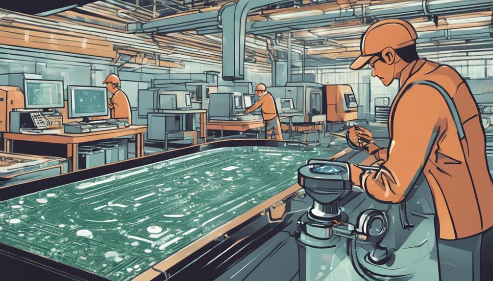
The typical PC fabrication process flow involves a series of precise and meticulous steps, from design and layout creation to final inspection and packaging, ensuring the production of high-quality printed circuit boards (PCBs) with excellent performance and reliability. The process begins with design and layout creation, followed by core material manufacturing, inner line processing, layering and drilling operations, panel plating and inspection, and copper plating and tin plating processes. As we explore each stage in greater detail, the complexities and nuances of PC fabrication will come to light, revealing the intricacies of this intricate process.
Key Takeaways
- The PCB fabrication process begins with design and layout creation using specialized software, followed by exportation in Gerber format.
- Core material manufacturing involves creating a fiberglass-reinforced epoxy resin composite with controlled thickness and composition for signal integrity.
- The inner line processing stage involves material coating, line pattern generation, and copper removal to create the desired circuit pattern.
- The layering and drilling operations stage involves bonding core boards with copper foil, precision drilling, and X-ray equipment for accurate positioning.
- The final stages include panel plating, copper plating, tin plating, and outer layer processing, followed by rigorous inspection and packaging.
Design and Layout Creation
During the initial stages of PCB fabrication, a critical step is the creation of a precise design and layout, which establishes the foundation for the entire manufacturing process. This stage involves using specialized PCB design software to create a detailed layout of the printed circuit board. The design must be meticulously crafted to guarantee that the final product meets the required specifications and performance standards.
Once the design is complete, it is exported in Gerber format, a standard file format used in the manufacturing process. This format provides a precise representation of the PCB's layout, allowing manufacturers to accurately fabricate the board.
To verify the design is feasible for manufacturing, Design for Manufacturability (DFM) checks are conducted to identify any potential issues that may arise during fabrication. By creating a precise design and layout, manufacturers can secure a high-quality PCB that meets the required specifications, paving the way for successful fabrication and manufacturing.
Core Material Manufacturing
The fabrication of printed circuit boards begins with the creation of the core material, an essential component that forms the foundation of the PCB, comprising fiberglass-reinforced epoxy resin and possessing specific properties that greatly impact the board's performance and reliability.
The core material is the base material for PCBs, and its manufacturing process involves cutting, stacking, pressing, and inspecting to guarantee uniformity and quality.
Key aspects of core material manufacturing include:
- Creating a fiberglass-reinforced epoxy resin composite with specific dielectric constant and thermal conductivity properties
- Controlling the core material's thickness and composition to meet design requirements for signal integrity and impedance control
- Implementing quality control measures to ensure consistent PCB characteristics and reliable electronic performance
- Maintaining uniformity in the core material to prevent variations in PCB performance
- Optimizing the core material's properties to meet specific application requirements
Inner Line Processing

In the inner line processing stage of PCB fabrication, the material coating process is a critical step that enables the creation of the circuit pattern on the inner layers. This process involves applying a photosensitive film onto the core board, which is then cured to define the desired circuit traces.
The line pattern generation process is also initiated at this stage, where the precise exposure times and solvent quantities are carefully controlled to achieve the required circuit design specifications.
Line Pattern Generation
Applying photosensitive film to copper layers initiates the line pattern generation process, a crucial step in forming accurate conductive paths on the inner layers of the printed circuit board (PCB). This process guarantees the precise formation of conductive paths, directly impacting the functionality and performance of the final PCB.
Here are the key aspects of line pattern generation:
- Photosensitive film is applied to copper layers to create a patterned mask
- The film is cured with UV light to create a hardened mask for etching
- The hardened mask protects the desired copper pattern during etching
- Excess copper is removed using a chemical solution, leaving behind the desired circuit pattern
- The resulting pattern is essential for the accurate formation of conductive paths on the inner layers of the PCB
Material Coating Process
During the material coating process, a photosensitive film called photoresist is meticulously applied to copper-clad laminate boards, paving the way for the precise reproduction of the circuit design on the inner layers of the printed circuit board. This process is a pivotal step in the fabrication of printed circuit boards (PCBs).
The photoresist is then exposed to UV light through a film mask, which transfers the PCB design onto the copper layer. The development process that follows involves using chemicals to remove the unexposed photoresist, leaving behind the copper traces that form the circuit pattern. This precise process ensures accurate reproduction of the circuit design on the inner layers of the PCB, which is essential for subsequent manufacturing processes.
The material coating process is a critical step in inner line processing, as it lays the foundation for the creation of the circuit pattern on the inner layers of the PCB. By accurately reproducing the circuit design, this process sets the stage for the successful fabrication of high-quality PCBs.
Layering and Drilling Operations

In the layering and drilling operations stage of PCB fabrication, precise control of layer thickness is crucial to guarantee the structural integrity of the board.
The hole drilling technique employed is also essential, as it directly impacts the quality of the electrical connections and component mounting.
As we examine the layering and drilling operations, we will focus on the key aspects of layer thickness control and hole drilling techniques that contribute to a reliable and functional PCB.
Layer Thickness Control
Layer thickness control in PCB fabrication is crucial and heavily dependent on precise drilling operations to ensure consistent copper thickness on each layer. This process involves bonding core boards with copper foil using prepreg material to guarantee uniformity in layer thickness. This precision is essential for securing signal integrity, impedance control, and overall performance of the PCB.
To achieve accurate layer thickness control, PCB fabrication utilizes computer-driven machines that create precision holes without damaging the layers or tearing the copper foil. Advanced techniques such as using X-ray equipment for positioning during drilling play a significant role in achieving precise layer thickness control.
Key aspects of layer thickness control in PCB fabrication include:
- Copper thickness control through precise drilling operations
- The layering process using prepreg material for uniformity
- Bonding core boards with copper foil for consistent thickness
- Maintaining signal integrity and impedance control through precise layer thickness
- Utilizing X-ray equipment for accurate positioning during drilling
Hole Drilling Techniques
Accurate hole drilling techniques are essential in PCB fabrication. They enable the creation of precise mounting holes for components and interconnections between layers. In this process, computer-driven machines are utilized for precision drilling, ensuring accurate hole placement and diameter.
To achieve this, X-ray equipment is employed to accurately position drill targets on the PCB layers during the drilling process. Additionally, Aluminum plates are often used to prevent tearing of the copper foil on the PCB layers, ensuring smooth drilling operations.
The drilling process is critical for creating interconnections between layers and components on multilayer PCBs. It ensures alignment of holes for proper component placement and electrical connections. By using precision drilling techniques, PCB fabricators can achieve precise hole diameters, enabling reliable electrical connections and component mounting.
This precise control over hole drilling is particularly important in multilayer PCBs, where accurate interconnections are essential for excellent performance.
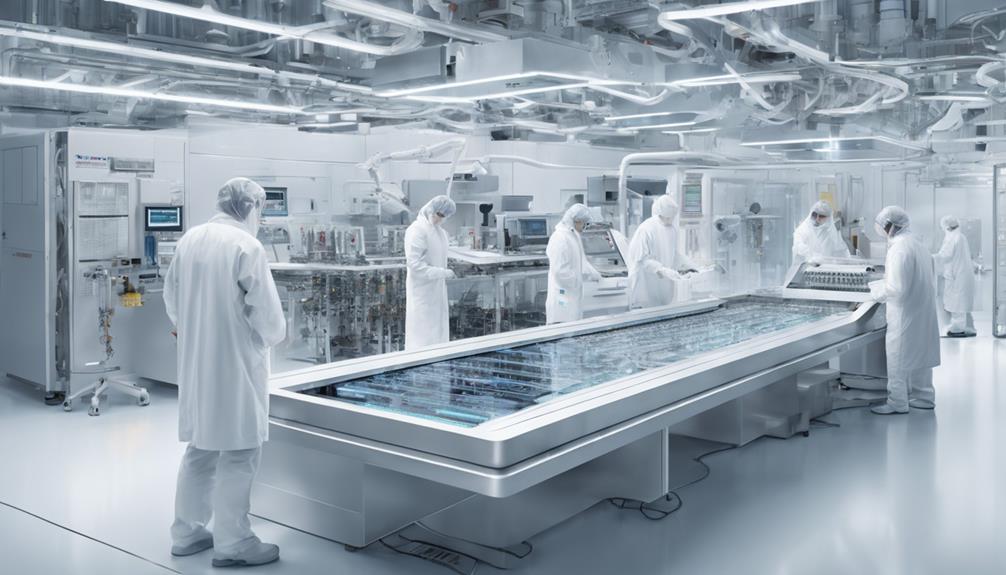
Panel Plating and Inspection

During the panel plating process, the entire panel is immersed in a copper plating bath to deposit a uniform layer of copper onto the surface of the panel, which is crucial for achieving peak conductivity and circuit performance. This copper layer serves as the foundation for the PCB's circuitry.
Copper plating is followed by tin plating to prevent oxidation and improve solderability.
The copper film thickness is meticulously monitored to guarantee uniformity and ideal conductivity.
Post-plating, the panel undergoes Automated Optical Inspection (AOI) to detect any defects or irregularities in the traces.
Outer layer processing involves applying solder mask, followed by cleaning processes, and adding the silk screen layer for essential PCB information.
Proper panel plating and inspection are crucial steps in the PC fabrication process, as they directly impact the overall quality and reliability of the final product.
Secondary Inspection and AOI
In the secondary inspection stage, Automated Optical Inspection (AOI) plays a critical role in detecting defects or errors in the PCB fabrication process.
To guarantee the quality and reliability of the final product, AOI systems employ advanced detection methods, including various inspection techniques and algorithms.
The component verification process is also an essential aspect of AOI, where the accuracy of component placement and orientation is meticulously checked against design specifications.
AOI Detection Methods
The AOI detection method, an essential secondary inspection technique in PCB fabrication, leverages advanced camera systems and sophisticated algorithms to identify a wide range of defects on both the top and bottom layers of the printed circuit board. This technology plays a critical role in guaranteeing the quality of PCBs by detecting defects such as missing components, misalignment, and soldering issues.
AOI systems offer several benefits, including:
- Improved accuracy: AOI systems reduce manual inspection errors, making sure that defects are detected accurately and efficiently.
- Enhanced production efficiency: AOI technology scans the entire PCB surface quickly, reducing production time and increasing overall efficiency.
- Comprehensive inspection: AOI systems inspect both the top and bottom layers of the PCB, making sure that defects are detected on all layers.
- Reduced manual inspection time: AOI systems automate the inspection process, reducing the need for manual inspection and freeing up resources for other tasks.
- Improved PCB quality: AOI technology helps guarantee that PCBs meet the required quality standards, reducing the risk of defects and improving overall product reliability.
Component Verification Process
Precision is paramount in the component verification process, where secondary inspection and AOI technology converge to guarantee the fabricated PCB aligns with the original design intent.
During this critical step, automated optical inspection (AOI) systems are employed to detect defects or errors in the PCB design. By leveraging cameras and advanced image processing algorithms, AOI systems compare the fabricated PCB against the original design files, identifying defects such as missing components, misalignments, soldering issues, or short circuits.
This meticulous inspection ensures the quality and reliability of the PCB, preventing defects from propagating to subsequent manufacturing steps. The component verification process through AOI is a crucial step in maintaining the integrity and functionality of the final PCB product.
Outer Layer Processing
During the outer layer processing stage, a solder mask is applied to safeguard the copper traces on the outer layers of the printed circuit board (PCB). This vital step guarantees the durability and functionality of the PCB during its operational lifespan.
Outer layer processing involves more than just applying a solder mask. It also includes:
- Cleaning processes to remove any contaminants and ensure proper adhesion of components
- Applying the silk screen layer to provide important information like component designators and logos on the PCB
- Ensuring the final finishing and protection of the board before it is assembled into electronic devices
- Guaranteeing the PCB's reliability and performance by protecting the copper traces from corrosion and damage
- Enhancing the overall quality and reliability of the PCB by ensuring a smooth and defect-free surface
Solder Mask Application

Following outer layer processing, the application of a solder mask is a critical step in protecting the copper traces and preventing solder bridges between components. The solder mask, typically green in color, is applied to the PCB surface using a screen printing process. This process provides insulation to prevent short circuits and corrosion, thereby enhancing the PCB's reliability and longevity.
| Benefits | Description |
|---|---|
| Insulation | Prevents short circuits and corrosion |
| Reliability | Enhances PCB's reliability and longevity |
| Solder Mask Clearances | Allows for component attachment during PCB assembly |
The solder mask application involves curing the applied material to ensure proper adhesion and durability. Openings in the solder mask, called solder mask clearances, allow for component attachment during the PCB assembly process. By applying a solder mask, the PCB's functionality and performance are safeguarded, safeguarding, ensuring optimal operation and extended lifespan. This critical step in the PC fabrication process flow plays an essential role in producing high-quality PCBs.
Silk Screen Printing Process

In the silk screen printing process, precise control over screen preparation and ink thickness is essential to achieve high-quality prints.
The screen preparation method employed can greatly impact the final print quality, with factors such as mesh count, emulsion thickness, and screen tension all playing a vital role.
Screen Preparation Methods
Silk screen preparation in PCB fabrication involves a meticulous process of creating the top and bottom layer identification marks, which are essential for component assembly and quality control. This process utilizes a mesh screen with a stencil of the PCB design to apply ink onto the board. The silk screen process adds labels, logos, component outlines, and other essential markings.
The following key aspects are critical for effective screen preparation:
- A durable, epoxy-based ink is used to guarantee long-term readability of the identification marks.
- The stencil of the PCB design is carefully created to ensure accurate reproduction of the design.
- Proper alignment and registration are vital for accurate silk screen printing on PCBs.
- The mesh screen is carefully cleaned and maintained to prevent defects and ensure consistent results.
- The silk screen process is closely monitored and controlled to achieve high-quality output.
Ink Thickness Control
During the silk screen printing process, maintaining precise control over ink thickness is vital to guarantee excellent PCB readability, durability, and functionality. Ink thickness control is imperative to make certain the uniform application of ink onto the PCB surface, which directly impacts the visibility of component labels, logos, and other critical information. Inadequate ink thickness can result in poor readability, compromised durability, and impaired functionality of the PCB.
To achieve precise ink thickness control, the silk screen printing equipment must be calibrated with utmost precision. This calibration ensures that the desired ink thickness is consistently maintained throughout the PCB fabrication process. Quality control measures are implemented to monitor and regulate ink thickness, ensuring that it meets the required standards.
The uniform application of ink also prevents copper oxidation, which can compromise the PCB's performance. By maintaining precise ink thickness control, manufacturers can guarantee high-quality PCBs that meet the required standards for readability, durability, and functionality. This critical step in the silk screen printing process is essential to producing reliable and efficient PCBs.
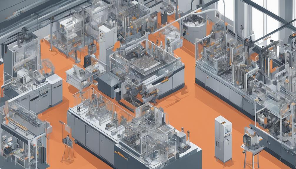
PCB Fabrication Techniques

By combining multiple processes, PCB fabrication techniques effectively transform raw materials into functional printed circuit boards. This involves a series of precise steps that guarantee high-quality output. These techniques encompass various stages that secure the production of high-reliability PCBs.
The PCB fabrication techniques involve:
- Inner layer preparation:
- Printing inner layers
- Applying photo resist
- Drilling holes
- Applying surface finish
- Layer alignment and inspection:
- Securing precise registration
- Defect detection
- Comparison with Gerber files
- Layer bonding and drilling:
- Using prepreg for bonding
- Computer-driven machines for drilling
- X-ray locators for spot identification
- Final production and inspection:
- Involving surface finish
- Quality assurance inspection
- Bonding press for layer bonding
- Imaging with PCB design
- Photo resist application
- Quality control:
- Securing that the final product meets the required standards and specifications
CCL Manufacturing Process

The CCL manufacturing process, a vital component of PCB fabrication, involves a series of precise steps that ultimately determine the signal transmission characteristics and impedance in printed circuit boards. This process is essential for guaranteeing signal integrity and reliability in PCBs.
The CCL manufacturing process begins with cutting and stacking core laminate materials, followed by pressing and inspection. The inner layer process involves applying photosensitive film, curing, and removing excess copper for circuit formation. Exposure times and copper solvent quantities vary based on the type of board being manufactured.
The quality of CCL manufacturing directly impacts the performance of the PCB, making it crucial to maintain high standards throughout the process. By controlling factors such as material selection, layer thickness, and processing conditions, manufacturers can optimize the CCL manufacturing process to achieve ideal signal transmission characteristics and impedance.
Laminates and Core Materials
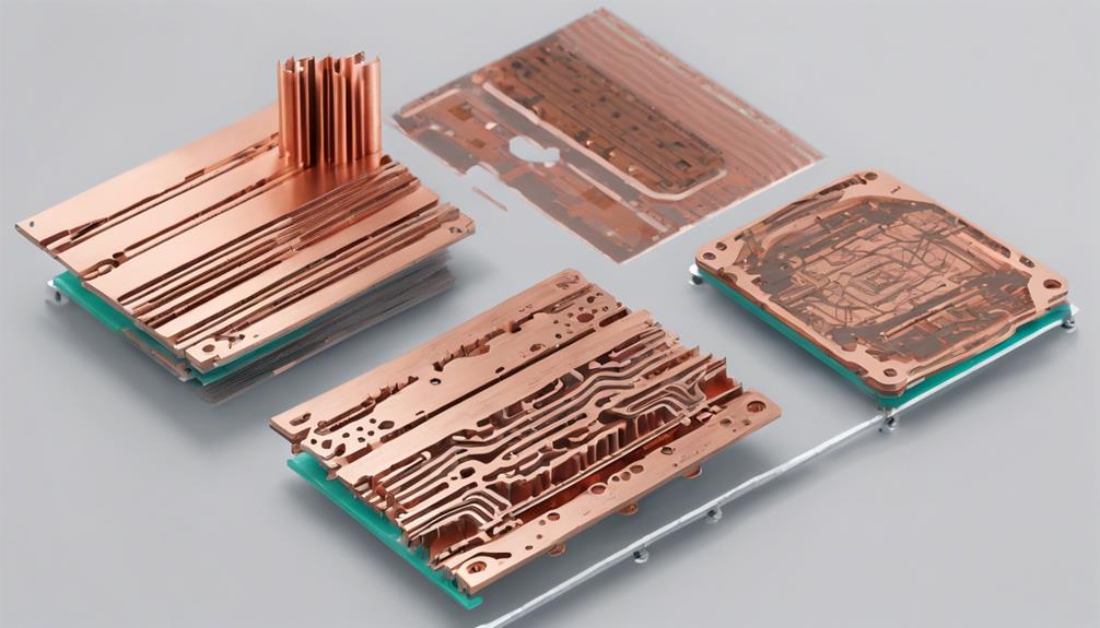
Forming the foundation of printed circuit boards, laminates comprise layers of core materials carefully selected for their mechanical strength, thermal properties, and electrical characteristics. These core materials, including epoxy resin and glass fiber, form the base structure of laminates used in PCB fabrication. The choice of core materials greatly impacts the PCB's overall performance, making it important to select materials that meet specific requirements.
Some key aspects of laminates and core materials in PCB fabrication include:
- FR-4, a popular core material, is chosen for its strength and insulation properties.
- Prepreg materials, such as resin-impregnated fiberglass sheets, ensure proper adhesion between core materials and copper foil.
- Aluminum plates are used during the drilling process to prevent tearing of the copper foil and ensure precise hole alignment.
- The combination of core materials and prepreg materials determines the PCB's mechanical strength, thermal properties, and electrical characteristics.
- The selection of core materials is vital to achieving optimal PCB performance and reliability.
Precision Drilling Techniques
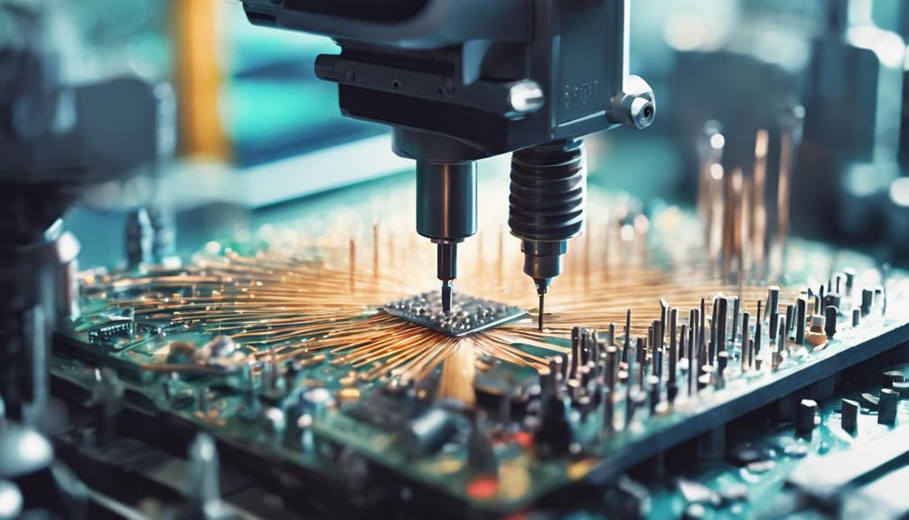
With the foundation of laminates and core materials in place, the precision drilling process plays an essential role in guaranteeing accurate hole placement and connectivity between layers in multilayer printed circuit boards. In the PCB fabrication process, precision drilling involves using computer-controlled machines to accurately drill holes for component placement. The drilling process is vital to secure alignment and connectivity between layers in multilayer PCBs.
| Drilling Technology | Hole Size | Application |
|---|---|---|
| CNC Drilling Machines | 0.1mm – 1.0mm | Through-hole components |
| Laser Drilling Technology | 0.01mm – 0.1mm | Microvias, high-density interconnect PCBs |
| CNC Drilling Machines with High-Speed Spindles | 0.05mm – 0.5mm | Fine-pitch components |
The drilling machines are programmed to follow the design layout provided in Gerber files to ensure precise hole placement. This accuracy is critical in PCB fabrication, especially for high-density interconnect PCBs and multilayer PCBs. By utilizing precision drilling techniques, manufacturers can achieve high-quality PCBs with reliable connectivity and performance.
Is the PC Fabrication Process Similar to Assembling Electronic Boards?
The PC fabrication process is not exactly similar to assembling electronic boards. While both involve the use of various components and soldering techniques, the visual process flow for electronic boards typically follows a different sequence and involves different materials and machinery.
Final Inspection and Packaging

Upon completion of the fabrication process, a rigorous final inspection is initiated to scrutinize the PCBs for defects, dimensional accuracy, and adherence to specifications. This stage is pivotal in guaranteeing the PCBs meet the desired quality standards.
Automated optical inspection (AOI) systems are commonly used for thorough inspection, leveraging advanced technology to detect even the slightest deviations.
Key aspects of the final inspection and packaging process include:
- Checking for defects, such as cracks, delamination, or shorts
- Verifying dimensional accuracy to ensure precise fit and functionality
- Confirming adherence to specifications, including material, thickness, and finish
- Protecting PCBs from environmental factors and physical damage during transportation
- Packaging PCBs in antistatic bags or foam-lined boxes for safe transit
Proper packaging is essential to ensure the PCBs reach the end user in pristine condition. By implementing these measures, manufacturers can guarantee high-quality PCBs that meet the required standards, ultimately leading to enhanced performance and reliability in the final product.
Frequently Asked Questions
What Are the 4 Stages of PCB Design Flow?
The four stages of PCB design flow are:
- Schematic capture involves creating a graphical representation of the circuit using specialized software.
- PCB layout is where components are placed and traces are routed on the board.
- Design verification validates that the design meets electrical and physical requirements.
- Design output produces Gerber files containing manufacturing data for PCB fabrication.
Each stage is vital in guaranteeing a functional and efficient printed circuit board.
What Are the 17 Common Manufacturing Processing Steps in PCB Production?
The 17 common manufacturing processing steps in PCB production encompass a wide range of activities. The process initiates with designing the PCB layout, followed by DFM checks and printing inner layers on laminate boards.
Subsequent steps involve layer alignment, bonding outer layers with substrate, drilling precision holes, and finalizing PCBs with surface finish. Stringent inspection processes, including automatic optical inspection and laser sensor scanning, guarantee defect-free production.
What Are the Steps Involved in PCB Fabrication?
The PCB fabrication process involves several intricate steps. Initially, the design layout is created, followed by a DFM check and plotting of photo films.
Inner layers are then prepared by printing, applying photo resist, drilling, and applying surface finish and solder mask. The layers are aligned and inspected using optical punch machines and laser sensors.
The outer layers are bonded, drilled, and plated with copper, culminating in final production and inspection for quality assurance.
What Is the Process Flow of PCB Assembly?
As the conductor orchestrates the symphony of components, the PCB assembly process unfolds. It begins with component preparation, where precision-crafted parts are carefully selected and organized.
Next, the automated assembly machines take center stage, accurately placing and soldering components onto the board with precision and speed.
The maestro of quality control, AOI, inspects the assembled PCB, ensuring harmony between form and function.
The final movement: functional testing, where the PCB is brought to life, its performance a proof of the symphony of assembly.