In high-frequency designs, component packaging is essential for ensuring signal integrity, minimizing electromagnetic interference, and maintaining reliable performance. Effective packaging prevents signal degradation and system failure by minimizing parasitics, optimizing thermal management, and utilizing advanced packaging techniques. Ceramic Quad FlatPack and Ball Grid Array packages offer exceptional thermal conductivity, electrical insulation, and compact size, making them suitable for RF and microwave applications. To navigate the complexities of high-frequency design, a thorough understanding of packaging considerations is important, and exploring these intricacies further reveals the nuances of design optimization and performance enhancement.
Key Takeaways
- Component packaging ensures signal integrity, minimizes electromagnetic interference, and maintains reliable performance in high-frequency designs.
- Ceramic Quad FlatPack and Ball Grid Array packages offer exceptional thermal conductivity, electrical insulation, and compact size for HF applications.
- Effective component packaging mitigates signal degradation, inductance, and capacitance issues, ensuring peak performance in high-frequency circuits.
- Proper packaging enables efficient thermal management, reducing thermal resistance and ensuring stable operation in high-frequency PCBs.
- Optimized component packaging enhances signal quality, reduces electromagnetic interference, and prevents system failure in high-frequency designs.
Importance of Component Packaging
In high-frequency designs, the packaging of components plays a pivotal role in ensuring signal integrity, minimizing electromagnetic interference, and maintaining reliable performance. The importance of component packaging lies in its ability to mitigate signal degradation and electromagnetic interference, thereby ensuring the overall functionality and reliability of high-frequency electronic systems.
On a printed circuit board (PCB), component packaging is critical in managing high-frequency signals, impedance matching, and heat dissipation. Effective packaging techniques help reduce electromagnetic interference, which is essential in high-frequency applications where signal integrity is paramount.
By optimizing component packaging, designers can minimize signal degradation, ensuring reliable performance and maintaining the integrity of high-frequency signals.
In high-frequency designs, the importance of component packaging cannot be overstated, as it directly impacts the overall performance and reliability of the system. By recognizing the significance of component packaging, designers can develop high-frequency systems that operate efficiently and reliably.
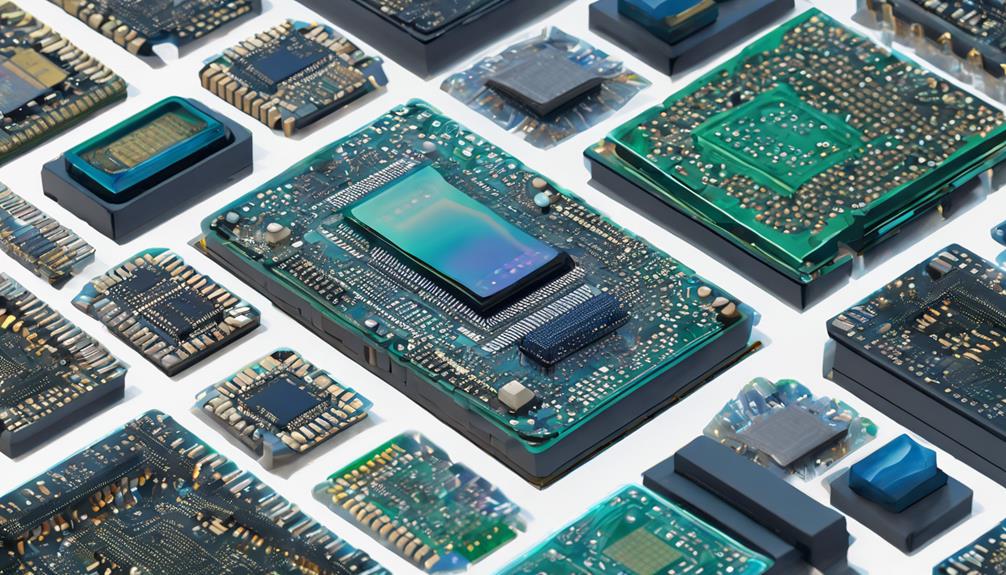
Component Packaging Types

In the field of high-frequency design, the selection of component packaging type plays a crucial role in achieving peak performance.
Two prominent packaging types that warrant consideration are Ceramic Quad FlatPack and Ball Grid Array, both of which offer unique advantages in terms of thermal management, signal integrity, and compact layouts.
A closer examination of these packaging types reveals their distinct characteristics and suitability for specific high-frequency applications.
Ceramic Quad FlatPack
Among the various component packaging types, Ceramic Quad FlatPack (CQFP) stands out for its exceptional thermal conductivity and electrical insulation properties, making it an attractive option for high-frequency designs.
The robust ceramic material used in CQFP packages provides excellent thermal conductivity, making them ideal for dissipating heat in high-power applications. Additionally, the packages offer good electrical insulation properties, reducing the risk of signal interference in high-frequency circuits. This makes CQFP a reliable choice for designers seeking to minimize signal degradation and guarantee dependable performance.
The flat, square shape of CQFP packages also allows for efficient use of PCB real estate, making them a popular choice in high-frequency electronic designs. Moreover, CQFPs are known for their durability and resistance to environmental factors, ensuring reliable performance in harsh operating conditions.
Ball Grid Array
Building on the advantages of ceramic quad flatpacks, ball grid array (BGA) packages have emerged as a popular component packaging type for high-frequency designs, offering enhanced thermal and electrical performance. BGA packages feature an array of solder balls on the bottom for electrical connections, providing a robust and reliable interconnect solution. This packaging type is particularly well-suited for RF and microwave applications, where high-frequency signal integrity is paramount.
| Characteristics | Benefits |
|---|---|
| High-density interconnects | Improved signal integrity |
| Enhanced thermal performance | Reduced thermal resistance |
| Array of solder balls | Robust electrical connections |
| Compact package size | Increased design flexibility |
BGA packages offer several advantages, including high-density interconnects, enhanced thermal performance, and compact package sizes. These benefits make BGA an attractive option for designers of high-frequency circuits, where signal integrity and thermal performance are critical. By leveraging the advantages of BGA packages, designers can create high-performance RF and microwave systems with improved reliability and reduced size.
Design Considerations for HF

High-frequency PCB designs necessitate a meticulous evaluation of various design parameters to mitigate signal degradation and guarantee peak performance. In high-frequency applications, signal routing, impedance discontinuities, and signal integrity are important considerations to ensure peak performance.
To achieve signal integrity in high-frequency PCBs, the following design considerations are essential:
- Controlled impedance: Maintaining a consistent impedance throughout the signal path is vital to prevent signal reflections and degradation.
- Optimized power distribution: A well-designed power distribution network is necessary to minimize power noise and guarantee stable operation.
- Material selection: Selecting materials with ideal electrical properties, such as low dielectric loss and high thermal conductivity, is critical for high-frequency performance.
- Signal routing techniques: Implementing techniques like fly-by topology in DDR4 configurations and minimizing signal reflections by avoiding trace bends are important for maintaining signal integrity.
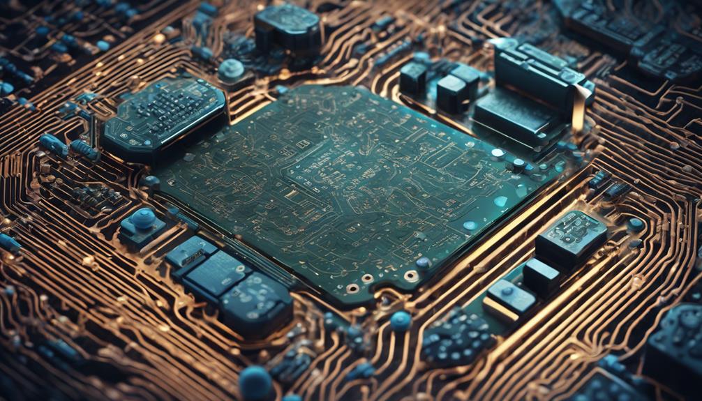
Signal Integrity and Parasitics

In high-frequency designs, signal integrity is only as reliable as the ability to mitigate the parasitic effects that can compromise it, making the management of inductive and capacitive elements a critical aspect of component packaging.
Signal integrity is essential for maintaining accurate and reliable communication in high-frequency designs. However, parasitics, such as inductance and capacitance, can greatly impact signal quality and performance, leading to signal distortion and compromised signal integrity.
To prevent signal distortion and maintain high-frequency operation, minimizing parasitics is vital. Careful design considerations are necessary to reduce parasitic effects and ensure excellent signal integrity.
Understanding and managing parasitics is key to achieving successful high-frequency component packaging. By mitigating parasitic effects, component packaging can guarantee accurate communication and reliable operation in high-frequency designs.
Effective management of parasitics enables the creation of high-performance components that can operate reliably at high frequencies, making it an important aspect of component packaging in high-frequency designs.
Grounding Strategies for HF

Proper grounding strategies are essential in high-frequency designs, as they play a critical role in reducing interference and signal degradation by providing a low-impedance path to ground for noise and interference currents. Effective grounding techniques are vital for maintaining signal integrity, reducing electromagnetic coupling, and minimizing signal degradation in high-frequency designs.
To achieve the best grounding strategies, consider the following:
- Separate digital and analog ground planes to reduce noise and crosstalk between digital and analog sections.
- Use ground reference points to connect different ground planes and minimize noise and crosstalk.
- Implement ferrite beads to control interference between digital and analog sections.
- Optimize ground plane layout to reduce electromagnetic coupling and signal degradation.
Thermal Management Techniques

While effective grounding strategies are essential for maintaining signal integrity, thermal management techniques play a complementary role in guaranteeing the reliable operation of high-frequency components by preventing overheating and subsequent performance degradation.
To achieve this, various thermal management techniques can be employed. Heat sinks, for instance, provide an efficient means of dissipating heat away from high-power components. Thermal vias, which are vertical holes in the PCB, also facilitate heat dissipation by providing a thermal path from the component to the heat sink.
Additionally, PCB layout optimization is vital to minimize thermal resistance and ensure efficient heat dissipation. The use of dielectric materials with high thermal conductivity further aids in heat dissipation within the package.
To validate the effectiveness of these techniques, thermal simulations and testing are essential. By simulating thermal performance, designers can identify potential hotspots and optimize their designs accordingly. Subsequent testing verifies the thermal performance of the design, ensuring stable performance and reliability of high-frequency components.
Manufacturing Considerations

In the domain of high-frequency component packaging, manufacturing considerations are critical to ensuring the performance and reliability of the final product. Two key aspects that warrant attention are material selection criteria and supply chain logistics, which have a direct impact on the overall quality and efficiency of the manufacturing process.
Material Selection Criteria
When designing high-frequency printed circuit boards, the careful selection of materials with ideal dielectric, thermal, and mechanical properties is essential to guarantee signal integrity and reliability. The choice of materials has a substantial impact on the performance of high-frequency components, and improper selection can lead to signal degradation and system failure.
To achieve peak performance, the following material selection criteria should be considered:
- Dielectric constant and loss tangent: Low dielectric constant materials like Rogers 4350B are preferred to minimize signal loss and maintain signal integrity.
- Thermal conductivity: High thermal conductivity materials aid in efficient heat dissipation in high-power applications.
- Coefficient of thermal expansion (CTE): CTE matching between materials ensures reliability and prevents solder joint failures.
- Stable properties across frequencies: Selecting materials with consistent properties across varying frequencies is essential for maintaining signal integrity in high-frequency designs.
Supply Chain Logistics
Efficient supply chain logistics play a critical role in high-frequency component packaging, as they directly impact production timelines, material quality, and ultimately, the reliability of the final product. In high-frequency design projects, supply chain logistics involve efficient material sourcing, handling, and transportation to meet production demands.
| Logistics Strategy | Benefits | Challenges |
|---|---|---|
| Just-in-Time Inventory Management | Minimizes storage costs, guarantees timely availability of packaging materials | Requires accurate demand forecasting, reliable suppliers |
| Collaborative Supply Chain Management | Enhances communication, reduces delays | Requires trust, shared goals among partners |
| Advanced Forecasting and Demand Planning | Optimizes inventory levels, prevents delays | Requires accurate data, sophisticated tools |
| Effective Communication | Ensures smooth operations, addresses disruptions | Requires clear protocols, regular updates |
| Strategic Material Sourcing | Guarantees quality, reduces costs | Requires thorough research, reliable suppliers |
Overcoming Packaging Challenges
By carefully selecting materials and optimizing component placement, designers can mitigate the adverse effects of packaging constraints on high-frequency designs. Overcoming packaging challenges is essential to guarantee signal integrity and minimize signal loss and interference.
To achieve this, designers can employ the following strategies:
- Optimize material selection: Choose materials with low dielectric loss and high thermal conductivity to reduce parasitic effects and thermal issues.
- Implement advanced packaging techniques: Utilize embedded passives, RF shields, and controlled impedance routing to minimize signal degradation and enhance signal integrity.
- Ensure effective thermal management: Implement heat sinks, thermal vias, and other thermal management techniques to prevent thermal issues that can compromise signal integrity.
- Employ proper grounding techniques: Use proper grounding and shielding techniques to minimize crosstalk and reduce electromagnetic interference.
Frequently Asked Questions
Can Component Packaging Affect Electromagnetic Interference (Emi) in HF Designs?
In high-frequency (HF) designs, component packaging plays a vital role in mitigating electromagnetic interference (EMI). The physical layout and construction of components can greatly impact EMI performance.
Poor packaging can worsen EMI issues, while optimized packaging can help minimize radiation and reduce noise coupling. As frequencies increase, even slight variations in packaging can have a profound impact on EMI, making careful component selection and packaging design essential for reliable HF operation.
How Do Different Packaging Materials Impact High-Frequency Signal Quality?
As the high-frequency signal navigates the labyrinth of component packaging, its quality hangs in the balance. The choice of packaging material plays a pivotal role in determining signal integrity.
Dielectric materials, such as ceramic or plastic, can introduce signal loss and dispersion, whereas metallic packages can induce electromagnetic interference.
In contrast, advanced materials like low-temperature co-fired ceramic (LTCC) or glass can minimize signal degradation, ensuring high-fidelity transmission.
What Is the Ideal Component-To-Board Gap for Optimal Signal Integrity?
The ideal component-to-board gap for peak signal integrity is a critical consideration in high-frequency design. A gap of 0.5 mm to 1.5 mm is generally recommended to minimize signal degradation.
This allows for effective electromagnetic shielding while maintaining a compact design. A smaller gap can lead to signal attenuation, while a larger gap can cause signal radiation.
Do Smaller Component Packages Always Provide Better High-Frequency Performance?
While smaller component packages often improve high-frequency performance by reducing parasitic inductance and capacitance, they do not always guarantee better results. In fact, smaller packages can introduce new challenges, such as increased thermal resistance and reduced power handling capabilities.
Additionally, the electrical performance of a component is influenced by internal construction, pinout, and materials, rather than package size alone.
Can 3D Packaging Improve Thermal Management in High-Frequency Designs?
'Measure twice, cut once' – a mantra that rings true in high-frequency design.
When it comes to thermal management, 3D packaging can be a game-changer. By stacking dies and integrating thermal interfaces, heat can be dissipated more efficiently, reducing thermal resistance and increasing power density.
This innovative approach enables higher frequency operations while minimizing thermal-related performance degradation, ultimately leading to enhanced overall system performance and reliability.