The PCB assembly process is a multifaceted sequence of precision-driven stages, encompassing component sourcing, fabrication, assembly, quality control, and packaging. Each stage demands meticulous execution to guarantee the manufacture of high-quality, defect-free printed circuit boards. The process begins with component sourcing, where careful selection and procurement of high-quality components are essential. Next, PCB fabrication involves etching, drilling, and plating, followed by precise component placement and solder paste application. Quality control and inspection stages detect defects and ensure proper functionality. As we explore each stage in detail, the intricacies of the PCB assembly process will be revealed, shedding light on the path to producing excellent printed circuit boards.
Key Takeaways
- The PCB assembly process involves multiple stages, including solder paste application, pick and place of surface mount components, and reflow soldering.
- Careful selection and procurement of high-quality components are crucial, considering factors like form factors and power requirements.
- Fabrication and assembly require precision, with attention to detail in etching, drilling, plating, and component placement aided by pick and place robots.
- Quality control and inspection are critical, utilizing methods like Automated Optical Inspection (AOI), functional testing, and visual inspection to detect defects and ensure functionality.
- Proper packaging and delivery procedures are essential, involving inspection, sturdy packaging materials, and reliable delivery methods to minimize transportation risks and ensure timely arrival.
PCB Assembly Process Overview
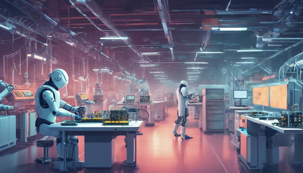
The PCB assembly process, a complex series of steps, sets the stage for transforming a bare board into a fully functional electronic device, demanding careful consideration of multiple factors to guarantee a high-quality end product.
This intricate process involves various stages, including solder paste application, pick and place of surface mount components, and reflow soldering. The quality assurance of the PCB assembly process relies heavily on the precision of each step, ensuring that the final product meets the required specifications.
A well-designed PCB layout is essential before initiating the assembly process, as it directly impacts the overall quality and reliability of the final product. Through-hole and surface-mount technologies are employed for component mounting, each with its unique advantages and challenges.
Component Sourcing and Preparation

Component sourcing, a critical precursor to PCB assembly, involves the careful selection and procurement of high-quality active and passive components that meet specific design requirements and specifications.
Active components, such as ICs, require power to function, whereas passive components, including resistors and capacitors, do not require power to operate in a circuit. The selection of components must also consider form factors, ensuring efficient placement and soldering during the assembly process.
Proper component preparation is equally important, as it directly impacts the overall performance and reliability of the assembled PCB. Component baking, a process that removes moisture, is a vital step in ensuring excellent component functionality and longevity.
The quality of sourced components significantly influences the overall reliability and functionality of the final PCB assembly. Hence, it is essential to source high-quality components that meet specific design requirements and undergo adequate preparation to ensure excellent performance and longevity of the assembled PCB.
PCB Fabrication and Assembly

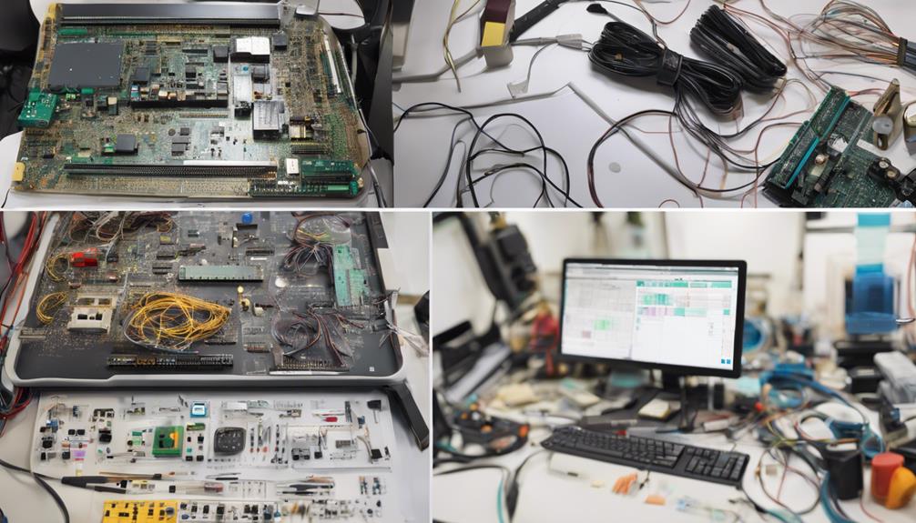
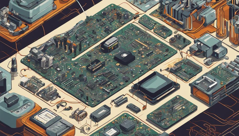
In the PCB manufacturing process, fabrication and assembly form a symbiotic relationship, with the former laying the groundwork for the latter by creating a solid foundation for component placement and soldering. Fabrication involves creating the actual printed circuit board (PCB) with copper traces and layers, while assembly focuses on adding components to the board for functionality.
The fabrication process includes etching, drilling, and plating to create the basic PCB structure, ensuring a vital foundation for component placement and soldering.
In the assembly process, components like resistors, capacitors, and ICs are precisely placed on the board using machinery like pick and place robots. Solder paste is then applied to the surface of the board, and the components are soldered to establish electrical connections.
Both fabrication and assembly are essential steps in creating a functional PCB, with each stage requiring attention to detail and adherence to specific manufacturing processes. By combining these two processes, electronic manufacturers can produce high-quality printed circuit boards that meet the demands of modern electronic devices.
Quality Control and Inspection

PCB assembly quality control and inspection protocols are essential gatekeepers, guaranteeing that only defect-free boards reach customers. These processes are vital in detecting defects and ensuring the reliability of printed circuit board (PCB) assemblies. Automated Optical Inspection (AOI) plays a significant role in quality control, using high-speed cameras to quickly detect defects in PCB assemblies. AOI reduces human error and enhances quality control by inspecting components, solder joints, and traces.
| Inspection Type | Description | Benefits |
|---|---|---|
| Automated Optical Inspection (AOI) | Uses high-speed cameras to detect defects | Reduces human error, enhances quality control |
| Functional Testing | Ensures proper functionality of PCB assemblies | Ensures reliability, detects functional defects |
| Visual Inspection | Human visual inspection of PCB assemblies | Detects cosmetic defects, verifies component placement |
In the PCB assembly process, quality control and inspection are critical in meeting performance standards and ensuring reliability. Early issue detection through quality control processes helps avoid costly recalls and improves customer satisfaction. By implementing these quality control measures, manufacturers can guarantee that only high-quality PCB assemblies reach customers, maintaining a reputation for excellence in the industry.
Can I Use the Same Assembly Process for PCB Manufacturing and Testing?
Yes, you can use the same assembly process for both PCB manufacturing steps and testing. By integrating the testing phase into the manufacturing process, you can streamline production and identify any defects early on. This can save time and resources in the long run.
Packaging and Delivery Procedures
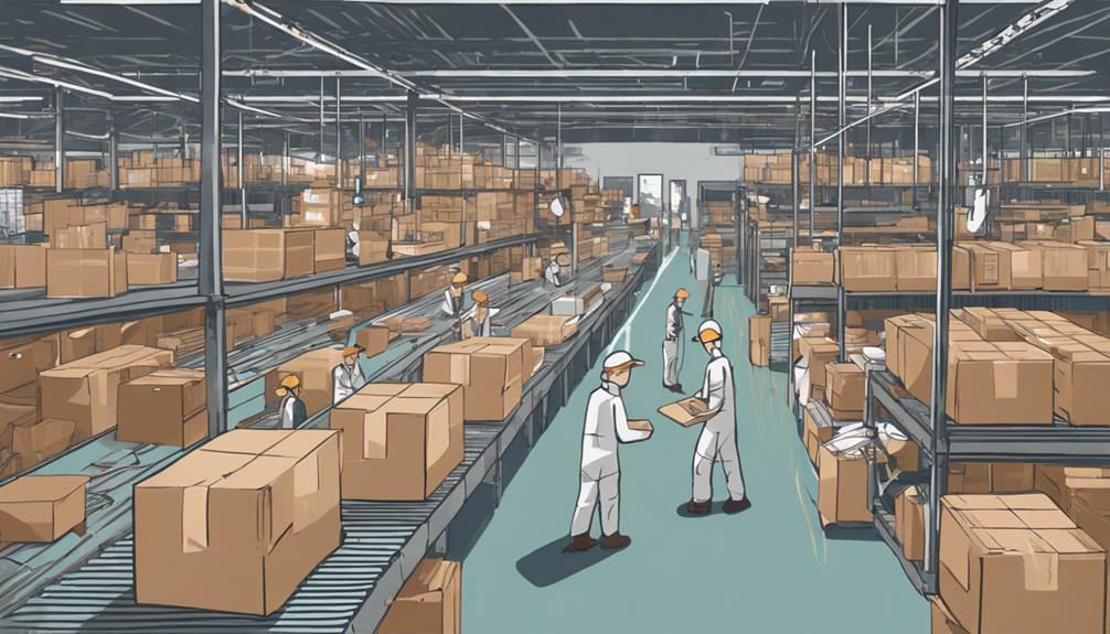
Following rigorous quality control and inspection protocols, the carefully assembled printed circuit boards are then prepared for safe transportation to their final destination through meticulously planned packaging and delivery procedures.
Inspection before packaging guarantees that any defects are addressed, preventing defective products from being shipped. Proper packaging procedures are vital in reducing the risk of damage to the assembled PCBs during transportation. Sturdy packaging materials are used to safeguard the PCBs, ensuring their integrity is maintained throughout the transportation process.
Reliable delivery methods are essential for PCBs to arrive at their final destination on time, guaranteeing the integrity of the final product. The packaging and delivery phase is a critical step in the PCB assembly process, as it directly impacts the quality of the final product. By minimizing the risk of damage during transportation, manufacturers can secure that their products meet the required standards, resulting in increased customer satisfaction and loyalty.
Frequently Asked Questions
What Are the Steps of PCB Assembly?
The steps of PCB assembly involve:
- Applying solder paste to the board.
- Precise component placement using robotic pick and place equipment.
Next,
- Reflow soldering melts the solder, creating secure connections.
Following that,
- Inspection and quality control procedures guarantee functionality and accuracy.
Finally,
- Through-hole insertion adds plated components, completing specialized soldering for specific applications.
Do You Have the Knowledge on the PCB Assembly Complete Process?
What does it take to guarantee a seamless PCB assembly process from start to finish?
To answer this, one must possess in-depth knowledge of the entire process. This encompasses every stage, from solder paste application and component placement to reflow soldering, inspection, and testing.
Effective quality control measures, efficient packaging, and timely delivery are also vital.
How Is a PCB Manufactured Step by Step?
The PCB manufacturing process involves a series of precise steps.
First, the PCB layout is designed using computer-aided design (CAD) software, followed by the creation of manufacturing files.
The substrate is then prepared, and copper patterning is applied.
Next, components are placed on the board using surface mount technology (SMT) or through-hole technology (THT).
Reflow soldering is then used to create electrical connections.
What Is the Process for Assembling Components Onto a PCB Board?
The process for assembling components onto a PCB board involves several meticulous steps. Initially, solder paste is applied to the board's designated areas.
Next, pick and place machines accurately position components, such as resistors and capacitors, onto the board.
Reflow soldering then bonds the components to the board.