Electronics in harsh environments require specialized packaging to guarantee reliable operation and prevent premature failure. Innovative approaches include IC, PCB, and optoelectronic packages, as well as MEMS and sensor packaging. Design considerations involve thermal management, stress mitigation, and material selection, with materials like silicon carbide and GaN offering enhanced thermal resistance. Advanced packaging technologies, such as hermetic ceramic packaging and wide-bandgap semiconductors, provide effective thermal management and high-frequency protection. By exploring these solutions, you can uncover the critical components of electronics protection in extreme environments.
Key Takeaways
- IC packages, PCB, and MCM packages protect electronics in harsh environments with innovative designs and materials.
- Wide-bandgap semiconductors like GaN and SiC provide high thermal conductivity and resistance to extreme temperatures.
- Advanced packaging technologies, such as hermetic ceramic packaging, ensure endurance in extreme conditions.
- Materials like high-quality plastics, sealed enclosures, and corrosion-resistant coatings are used to protect electronics from environmental damage.
- Effective thermal management, low inductance, and shock and vibration resistance are key considerations for packaging in harsh environments.
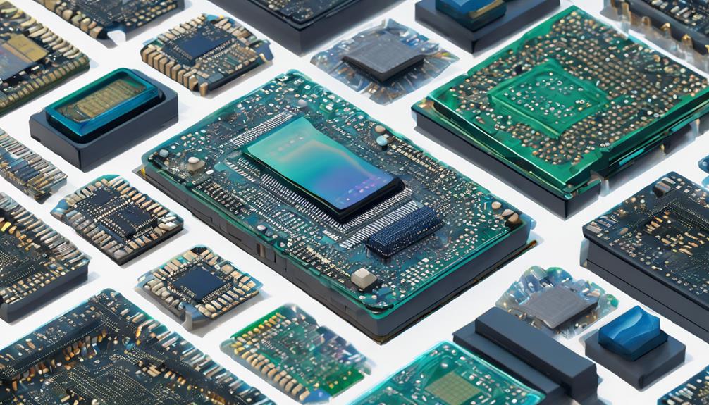
Electronic Component Packaging Types
Among the diverse range of electronic component packaging types, five primary categories stand out for their distinct roles in safeguarding electronic components in various applications and environments. These packaging types are essential for protecting electronic components in harsh environments, where reliability and durability are paramount.
IC packages are designed to protect integrated circuits, while PCB and MCM packages safeguard printed circuit boards and multi-chip modules.
Optoelectronic packages cater to optical and electronic devices, ensuring seamless interaction between light and electronics.
MEMS and sensor packaging protect microelectromechanical systems and sensors, which are critical in applications such as aerospace and industrial automation.
Finally, wafer-level packaging involves packaging semiconductor devices at the wafer level, enabling compact form factors while ensuring protection and functionality.
The development of advanced packaging technology has enabled the creation of robust and reliable electronic components capable of withstanding harsh environments. By understanding the unique strengths of each packaging type, designers and engineers can select the best packaging solution for their specific application, ensuring the reliable operation of electronic components in even the most demanding environments.
Designing for Extreme Temperatures
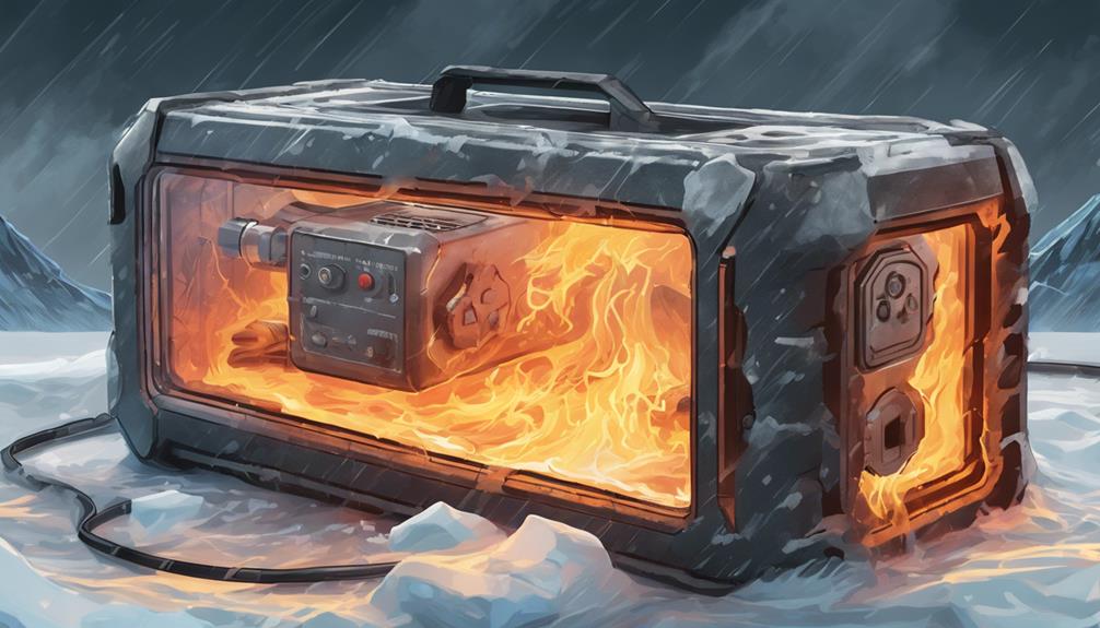
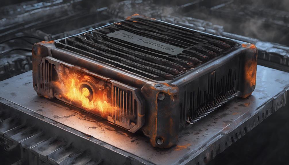
Designing electronics to operate reliably in extreme temperatures exceeding 300°C requires careful consideration of packaging solutions that can withstand thermal stresses and guarantee component integrity. High-temperature electronics (HTEs) demand innovative packaging approaches to ensure peak performance under harsh conditions. Materials like silicon carbide (SiC) are being explored for HTEs protection, offering enhanced thermal resistance and mechanical strength.
In addition to high-temperature resistance, packaging solutions must address challenges of exposure to shock, vibration, and acceleration in extreme conditions. This is particularly vital for applications like remote sensing, control, and actuator electronics near heat sources. Effective packaging electronics in these environments requires a deep understanding of thermal management, mechanical stress mitigation, and material selection.
Compliance with US Export Control Laws is also an important consideration for packaging electronics in harsh environments. By prioritizing these factors, designers can develop reliable and efficient electronics capable of withstanding extreme temperatures, ensuring top-notch performance in demanding environments.
High-Frequency Protection Methods

In high-frequency electronic packaging, the deployment of wide-bandgap semiconductors such as gallium nitride (GaN) and silicon carbide (SiC) has emerged as an essential strategy for mitigating the adverse effects of harsh environments. These materials are chosen for their ability to operate at high frequencies and temperatures where traditional electronics may fail.
The use of simulation tools like COMSOL enables the analysis of thermal and electrical responses of high-frequency electronic packaging designs, facilitating the optimization of material selection and thickness. This optimization helps reduce thermal resistance and inductance in high-frequency electronic packaging.
Innovative packaging designs aim to provide better thermal management and performance for electronics operating in extreme environments. By leveraging wide-bandgap semiconductors, designers can develop robust and reliable high-frequency electronic packaging solutions that can withstand the rigors of harsh environments.
Effective thermal management is critical in these designs, as it directly impacts the overall performance and reliability of the electronics.
Thermal Management Solutions
Effective thermal management is paramount in high-frequency electronic packaging, as it prevents overheating and guarantees peak performance in harsh environments. Thermal management solutions in electronic packaging focus on controlling heat to ensure peak performance in extreme conditions. This is essential, as overheating can lead to component failure and reduced lifespan.
Materials with high thermal conductivity, such as gallium nitride (GaN) and silicon carbide (SiC), are essential for efficient heat dissipation. Design considerations for thermal management involve selecting materials with low thermal resistance and optimizing layer thickness. The goal is to minimize thermal resistance and maximize heat transfer.
Innovations in thermal management aim to reduce inductance, improve efficiency, and enhance the performance of electronic components in extreme conditions. By optimizing thermal management, electronic components can operate reliably in harsh environments, ensuring peak performance and extended lifespan.
Effective thermal management is critical in high-frequency electronic packaging, and manufacturers must prioritize this aspect to deliver reliable and efficient electronic components.
Low-Inductance Packaging Options

When it comes to low-inductance packaging options, designers can leverage shielded metal packages that minimize electromagnetic interference and reduce signal degradation.
Alternatively, ceramic-based solutions offer a robust and reliable alternative, providing a hermetic seal that protects sensitive electronics from harsh environmental conditions.
Shielded Metal Packages
Shielded metal packages, engineered with advanced materials like gallium nitride and silicon carbide, have emerged as a preferred low-inductance packaging solution for high-frequency and high-temperature electronics operating in harsh environments. These packages offer robust performance in extreme conditions, owing to the unique properties of GaN and SiC.
Design considerations focus on minimizing thermal resistance and optimizing layer thickness for efficient thermal management. Simulation tools like COMSOL aid in analyzing thermal and electrical responses to enhance package design. By leveraging these advanced materials and design techniques, shielded metal packages provide improved inductance and thermal management capabilities, surpassing industry standards for performance.
This results in enhanced reliability and reduced signal degradation, making them an ideal solution for demanding applications. Additionally, the low-inductance characteristics of shielded metal packages enable high-frequency electronics to operate at efficient levels, even in extreme temperatures and environmental conditions.
Ceramic-based Solutions
What specific requirements must ceramic-based packaging solutions meet to guarantee reliable operation in harsh environments, where traditional electronics often fail? To answer this, let's explore the advantages of ceramic-based solutions.
Ceramic-based packaging solutions offer a unique set of benefits that enable reliable operation in extreme conditions. These packages are designed to withstand harsh conditions, such as high temperatures and high-frequency environments, where traditional electronics may fail.
| Characteristics | Benefits | Applications |
|---|---|---|
| Low Inductance | High-frequency operation | Aerospace, Defense |
| High Thermal Conductivity | Efficient heat dissipation | Industrial, Automotive |
| Superior Thermal Management | Optimal performance, longevity | Medical, Energy |
| High Reliability | Resilience in harsh conditions | Aerospace, Industrial |
| Low Parasitic Inductance | High-speed data transfer | Data Centers, Telecom |
These ceramic-based solutions are ideal for applications requiring high reliability and resilience in challenging operating conditions. By leveraging their unique properties, ceramic-based packaging solutions guarantee top-notch performance and longevity of electronic components, even in the most demanding environments.
High-Thermal Conductivity Materials

Among the key components in safeguarding electronics in harsh environments, high-thermal conductivity materials stand out for their pivotal role in maintaining peak performance.
These materials, such as gallium nitride (GaN) and silicon carbide (SiC), are wide-bandgap semiconductors that excel in withstanding extreme temperatures and high frequencies. Their exceptional thermal conductivity enables effective heat dissipation, a critical factor in ensuring peak performance in challenging conditions.
In designing packaging solutions for electronics exposed to harsh environments, selecting materials with high thermal conductivity is essential. GaN and SiC play a significant role in enhancing thermal management and overall reliability of electronics in extreme operating conditions.
The high thermal conductivity of these materials allows for efficient heat transfer, reducing the risk of overheating and subsequent component failure. By incorporating high-thermal conductivity materials into packaging designs, electronics can operate reliably in environments with extreme temperatures, vibrations, and humidity.
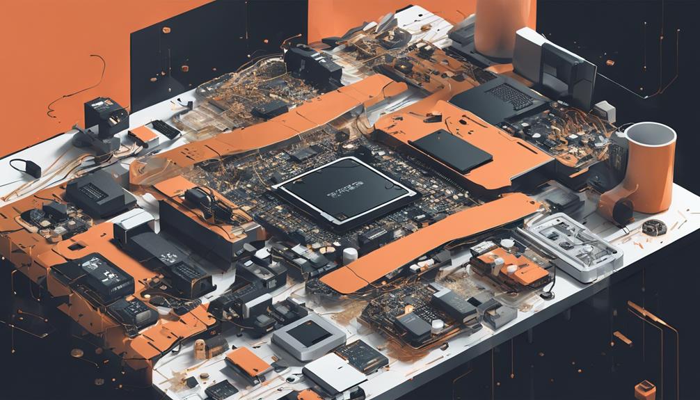
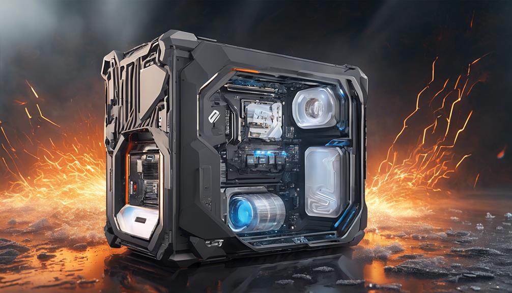
Innovative Packaging Designs

As electronics operating in harsh environments face increasingly demanding performance requirements, innovative packaging designs have emerged as an essential factor in guaranteeing reliable operation and minimizing downtime. The electronics industry is shifting towards advanced packaging solutions that prioritize thermal management and efficiency.
These innovative designs consider factors such as power and energy density, cost, and customer safety to create versatile, small, and easy-to-configure packages. With a focus on low inductance and high thermal conductivity, these designs are revolutionizing the protection of electronics in extreme conditions.
By controlling thermal management and increasing efficiency, these innovative packaging designs enable reliable operation in harsh environments. This is critical for the electronics industry, where equipment failure can have significant consequences.
GaN and SiC in Packaging
In GaN and SiC-based packaging, effective thermal management strategies are essential to guarantee reliable operation in harsh environments.
The selection of materials with ideal thermal conductivity, specific heat capacity, and thermal expansion coefficients is vital to mitigate thermal stress and ensure component longevity.
Thermal Management Strategies
High-power electronic packaging in harsh environments relies heavily on effective thermal management strategies, which involve the strategic selection of materials and design optimization to minimize thermal resistance and guarantee efficient heat dissipation.
Wide-bandgap semiconductors like gallium nitride (GaN) and silicon carbide (SiC) play an essential role in thermal management strategies, offering superior thermal conductivity and high-temperature tolerance. By leveraging these materials, innovative power modules can be designed to excel in extreme environment applications.
For instance, APEI's power modules utilizing GaN and SiC exhibit low inductance, high thermal conductivity, and superior thermal management capabilities. COMSOL software analysis has been instrumental in optimizing thermal and electrical responses in these designs, surpassing industry standards in thermal resistance and inductance.
Material Selection Criteria
When selecting materials for packaging in harsh environments, the primary criteria involve optimizing thermal resistance and inductance to guarantee reliable performance, making GaN and SiC attractive options due to their exceptional thermal conductivity and high-temperature tolerance.
These wide-bandgap semiconductors are chosen for their resilience in harsh environments, where traditional materials may fail. GaN modules excel in low inductance, facilitating rapid switching, while SiC modules are suitable for high currents and thermal loads.
Effective material selection is essential to ensure reliable performance in harsh environments. Advanced simulation tools, such as COMSOL, aid in analyzing thermal and electrical responses to optimize material selection for effective packaging solutions.
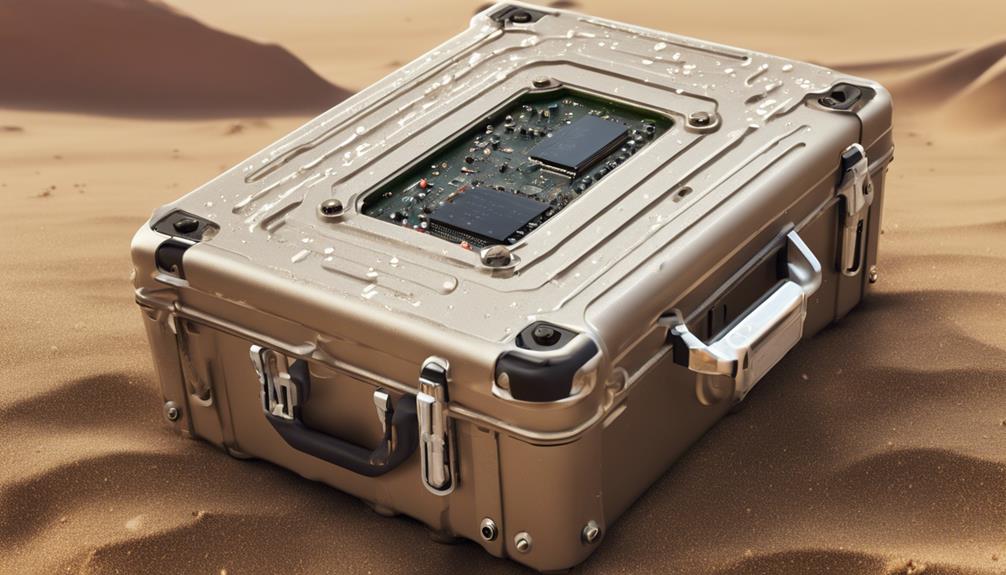
Challenging Environmental Factors

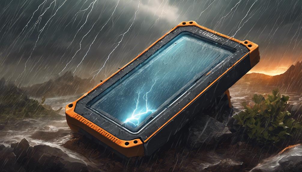
Environmental stressors, including extreme temperatures, moisture, humidity, dust, particulates, and potential submersion, pose significant threats to the reliability and longevity of electronic components in harsh environments. These environmental factors can lead to malfunctions, reduced lifespan, and potential failure of electronic components. Effective packaging solutions must consider temperature variations, protection from moisture and dust, and mechanical durability to guarantee the reliability of electronic components.
| Environmental Factor | Impact on Electronic Components |
|---|---|
| Extreme Temperatures | Malfunctions, reduced lifespan |
| Moisture and Humidity | Corrosion, electrical shorts |
| Dust and Particulates | Ingress, mechanical failure |
Design considerations for harsh environments involve selecting materials with high chemical resistance, thermal stability, and effective thermal management. Standards like Ingress Protection (IP) ratings and MIL-STD-810G testing ensure electronics are protected and reliable in challenging conditions. By understanding the challenging environmental factors and designing effective packaging solutions, electronic components can operate reliably in harsh environments, ensuring peak performance and extended lifespan.
Advanced Packaging Technologies

Advanced packaging technologies, such as hermetic ceramic packaging, have emerged as a vital solution for protecting electronics in harsh environments, offering high-temperature integrated circuits and withstanding extreme conditions. These innovative solutions are designed to guarantee the reliability of electronics in environments with high temperatures, shock, and vibration.
Some key features of advanced packaging technologies include:
- High-temperature integrated circuits for dependable operation in extreme conditions
- Withstanding extreme conditions through stringent qualification tests like MIL-STD-883
- Thermal management design strategies for enhanced efficiency and performance
- Use of wide-bandgap semiconductors like GaN and SiC for high-frequency and high-temperature applications
- Optimized design strategies for improved thermal resistance, low inductance, and enhanced capabilities
Reliable Operation in Extremes
Operating reliably in extreme environments demands innovative packaging solutions that can withstand harsh temperatures, mechanical stresses, and other adverse conditions.
Hermetic packaging, for instance, guarantees reliable operation of microcircuits in harsh environments by providing protection against extreme temperatures and mechanical stresses.
Advanced semiconductor materials like silicon carbide (SiC) are used to withstand high temperatures exceeding 300°C in applications near heat sources.
In oil and gas drilling, high-reliability electronics can endure extreme heat exposure of up to +250°C and mechanical stresses of 30,000g.
Innovative packaging designs, such as those from Global Circuit Innovations, extend standard microcircuit lifetimes by 10,000 times, making them ideal for downhole drilling and Department of Defense applications.
APEI's power packaging designs offer improved thermal management capabilities and low inductance for reliable operation in extreme environments.
Frequently Asked Questions
What Is the Best Packaging for Electronics?
When selecting the best packaging for electronics, hermetic ceramic packaging stands out for its high reliability and durability.
Conformal coatings, such as acrylic and parylene, provide additional protection against moisture and chemicals.
For extreme temperature applications, advanced semiconductor materials like silicon carbide (SiC) are essential.
Specialized packaging solutions from companies like SCHOTT offer tailored options for rugged environments, ensuring longevity and reliability in demanding conditions.
What Are the Levels of Electronic Packaging?
As we explore the world of electronic packaging, a hierarchical structure emerges, comprising four distinct levels. Like a meticulously crafted orchestra, each level harmoniously contributes to the symphony of protection.
The component level shields individual parts, while the PCB level integrates components onto a circuit board.
The module level combines multiple components, and the system level integrates modules into a final product. Each level plays an important role in ensuring the reliability and durability of electronic devices.