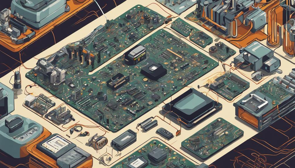
To successfully manufacture a printed circuit board (PCB) prototype, beginners must follow a meticulous step-by-step process. It begins with creating a precise schematic design, then designing the PCB stackup, and defining critical design rules. Collaboration with experienced engineers optimizes the design for manufacturability and cost-effectiveness. The fabrication process involves etching and laminating layers, drilling and plating the PCB, and applying solder mask and silk screen. Surface finishing and profiling, PCB assembly, and final quality checks and packaging complete the process. By following these steps, a reliable and efficient PCB prototype can be produced, and the nuances of each stage will be revealed as you explore further.
Key Takeaways
- Create a precise schematic design to serve as a blueprint for PCB layout and component connectivity.
- Plan PCB stackup carefully to ensure signal integrity, impedance control, and thermal management.
- Define design rules to govern PCB layout for signal integrity, manufacturability, and reliability.
- Collaborate with experienced engineers to optimize design for manufacturability and cost-effectiveness.
- Ensure quality control measures, including testing and inspection, to guarantee a reliable and efficient final product.
Understanding PCB Design Basics
At the core of PCB prototype manufacturing lies a thorough understanding of PCB design basics. This involves the intricate process of creating a schematic, layout, and component placement on a flat conducting plate. A well-designed PCB is important for ensuring manufacturability, cost-effectiveness, and peak performance.
To achieve this, it is essential to take into account key factors such as board size, trace width, materials, and environmental factors that may impact the PCB's functionality. Working with experienced engineering experts from the outset enables the identification of potential design flaws and ensures that the final product meets the required specifications.
Effective communication with PCB engineers is crucial in reducing the need for major revisions and project delays. Moreover, selecting a reputable PCB provider with extensive engineering experience guarantees a successful design that meets the desired standards.
Creating a Schematic Design

As the foundation of a successful PCB prototype lies in a well-crafted schematic design, it is crucial to create a precise and accurate visual representation of the circuit. A schematic design serves as a blueprint for the PCB layout, guaranteeing proper component placement and connectivity.
Utilizing design software such as Altium, Eagle, or KiCad, components are accurately placed, connected, and annotated to confirm clarity. This visual representation of the circuit allows designers to verify the functionality and connectivity of the components before proceeding to the PCB layout stage.
A well-crafted schematic design ensures that the PCB prototype functions as intended, reducing errors and costly reworks. By creating a precise schematic design, designers can confidently proceed to the PCB layout stage, knowing that their design is sound and reliable.
With a solid schematic design in place, the foundation is set for a successful PCB prototype.
Designing the PCB Stackup
The PCB stackup, an essential component of the PCB prototype, demands meticulous planning and design to guarantee peak performance, reliability, and manufacturability. A well-designed PCB stackup is vital for excellent signal integrity, impedance control, and thermal management. The layer order, signal routing, power distribution, and ground planes are all critical elements that must be carefully considered. The number of layers, material types, and thickness must be determined to ensure peak performance.
Proper PCB stackup design enhances electrical performance, EMI/EMC compliance, and manufacturability of the PCB prototype. It is essential to work closely with PCB designers and manufacturers to ensure the stackup design meets the project requirements and specifications. A carefully planned PCB stackup design ensures that the final product is reliable, efficient, and meets the desired performance standards.
Defining Design Rules

With a well-designed PCB stackup in place, attention turns to defining the design rules that will govern the PCB layout, guaranteeing that the prototype meets the required standards for signal integrity, manufacturability, and reliability.
These design rules define constraints for the PCB layout, including trace width, spacing, and via sizes, which are set based on the PCB manufacturer's capabilities and the intended application of the prototype. By following these design rules, issues such as signal interference, short circuits, and manufacturing errors can be prevented.
Design rules are essential in ensuring signal integrity, manufacturability, and reliability of the PCB prototype. They dictate the minimum and maximum values for trace width, spacing, and via sizes, among other parameters.
A design rule check (DRC) software is used to validate compliance with the specified design rules before fabrication. This ensures that the PCB layout is free from errors and meets the required standards.
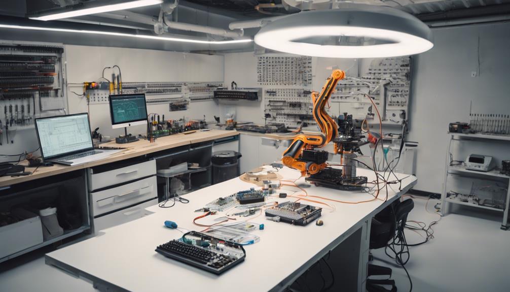
Working With Experienced Engineers

Collaborating with experienced engineers proves essential in maneuvering through the complexities of PCB prototype manufacturing, as their expertise can greatly enhance the overall design and manufacturing process. By working with experienced engineers, designers can optimize their design for manufacturability and cost-effectiveness, ensuring that the final prototype meets the required specifications and budget constraints.
| Benefits | Description |
|---|---|
| Efficient Troubleshooting | Identify and resolve design flaws and manufacturing issues promptly |
| Higher Quality Prototypes | Reduced errors and defects, resulting in a more reliable final product |
| Innovative Solutions | Expertise in finding creative solutions to complex design and manufacturing challenges |
| Faster Turnaround Times | Expedited prototype development and production, reducing time-to-market |
| Design for Manufacturability | Optimized design for easy and cost-effective production |
Choosing a Reputable PCB Provider

Choosing a reputable PCB provider is crucial, as it directly impacts the quality and timeliness of your prototype manufacturing process. A reliable provider can make all the difference in guaranteeing your project's success.
When selecting a PCB provider, look for engineering expertise to secure manufacturability and efficiency. Reputable providers offer design review services to identify errors early and prevent delays. Consider the provider's experience in handling various PCB types, such as rigid, flex, and rigid-flex circuits.
If you need rapid prototyping and fast turnaround times, choose a provider with quick turn services. Additionally, verify that the provider adheres to industry standards like IPC or MIL specifications for quality assurance. A reputable provider will have a proven track record of delivering high-quality PCBs on time.
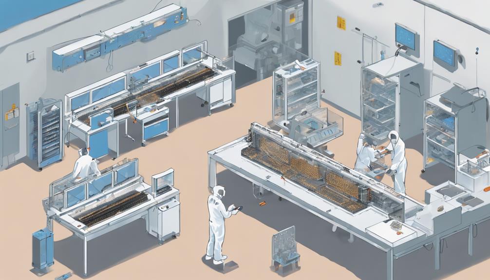
The PCB Manufacturing Process

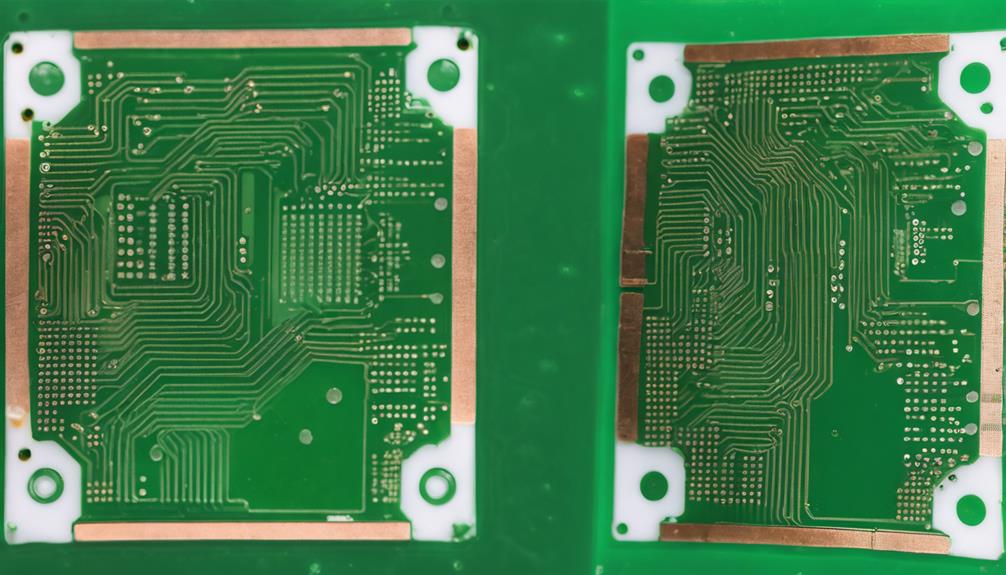
The PCB manufacturing process commences with the imaging of inner layers, where copper traces and circuits are meticulously created using films, marking the inception of a complex series of steps that ultimately yield a completed PCB prototype.
The next important step involves etching and drilling to remove unwanted copper and create holes for component placement. A solder mask is then applied to guarantee the PCB from environmental factors, followed by UV light blasting to harden the photoresist layer. Layer alignment and inspection guarantee precise alignment of inner and outer layers, with defects detected using automated optical inspection.
In the subsequent stages, outer layers are laminated, and a surface finish is applied. Finally, quality checks are conducted to verify the manufactured PCB prototype meets the design specifications. Throughout the process, precision and attention to detail are paramount to produce a high-quality printed circuit board that meets the design requirements.
Imaging and Printing Inner Layers
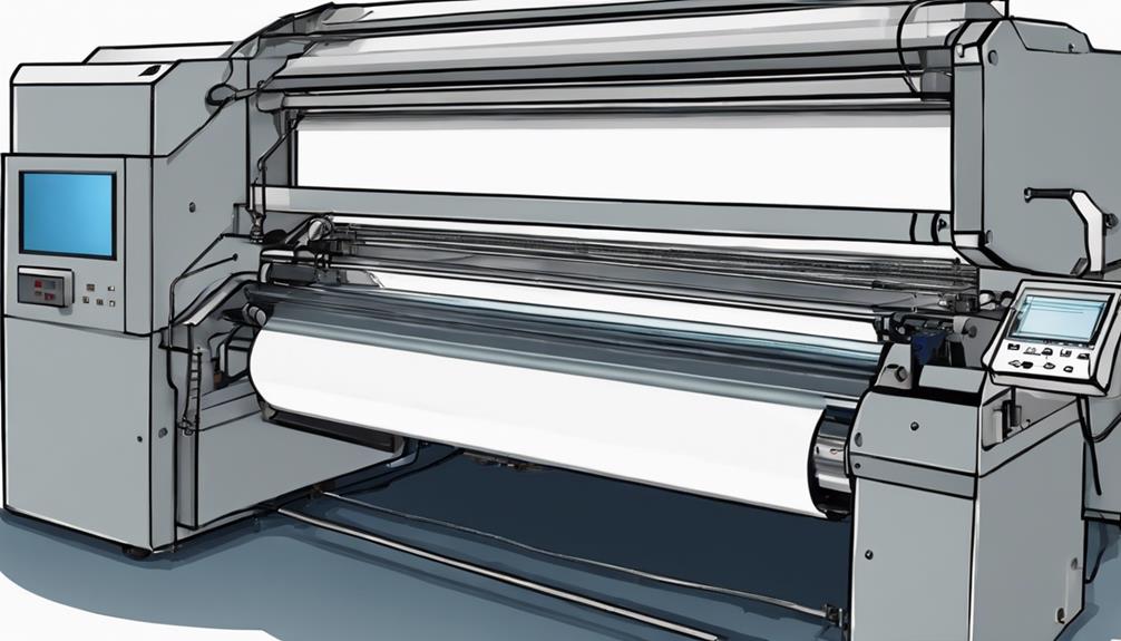
Inner layer imaging, a vital step in the PCB manufacturing process, involves the precise printing of circuit patterns and component placement onto films using a plotter printer. This process converts design files into physical representations of the inner layers, which are essential for accurate circuit connections and component positioning.
The films created during imaging represent copper traces, circuits, and component placement on the inner layers, providing a precise blueprint for subsequent manufacturing steps.
The printing process employs a combination of clear and black ink to define the layout, ensuring precise registration and accuracy. The black ink defines the copper traces and component placement, while the clear ink provides a transparent background.
The printed films are then stored for future reference and use in the PCB manufacturing process. The precision of the imaging and printing process is vital, as any errors or inaccuracies can lead to faulty circuit connections and component malfunctions.
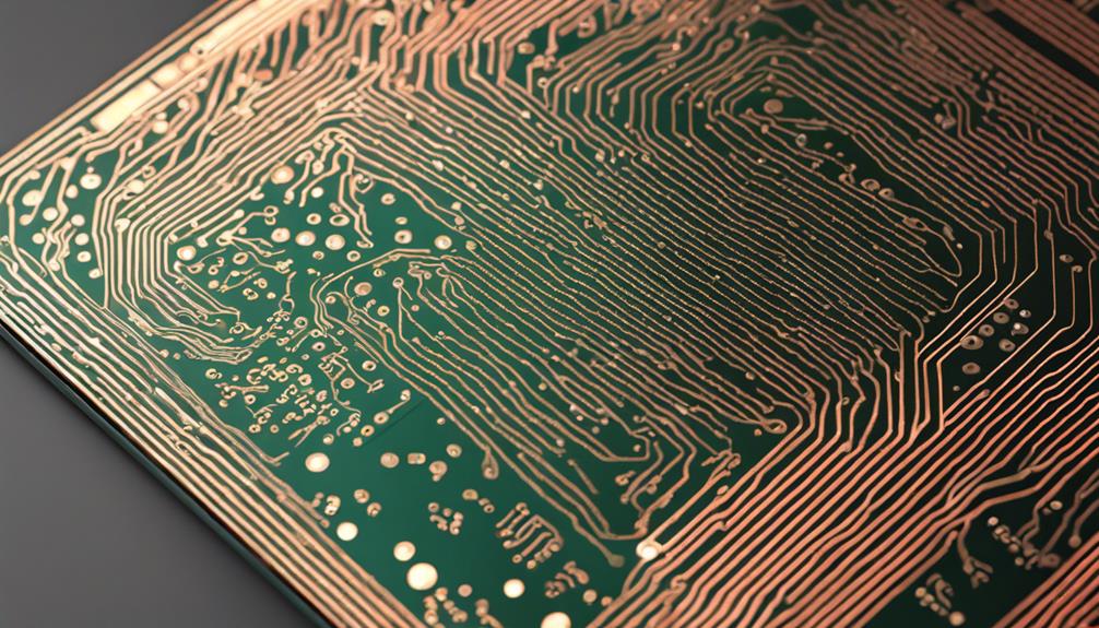
Etching and Laminating Layers
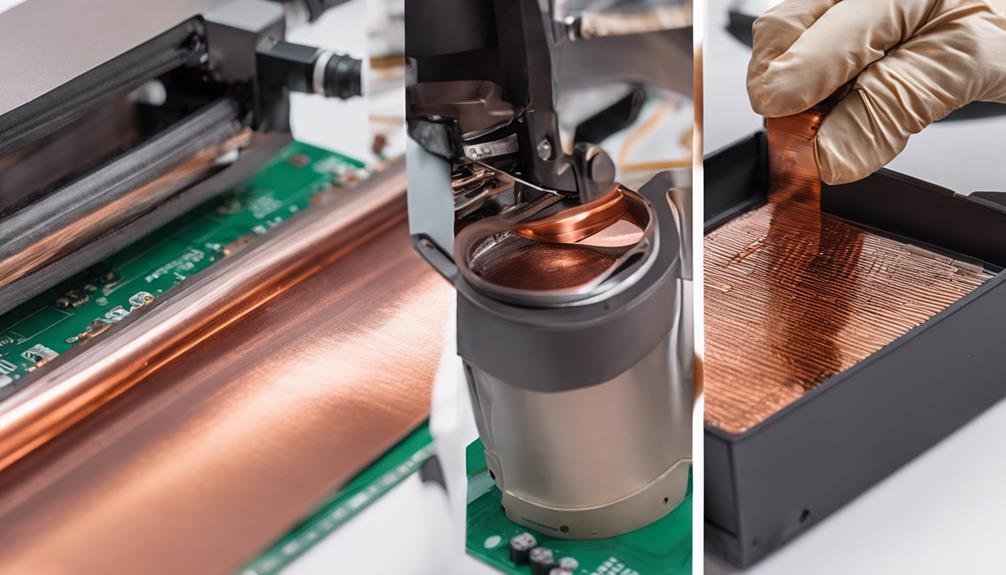
In the etching and laminating layers stage of PCB prototype manufacturing, several critical processes come into play. Here, we will explore the various etching techniques used to remove excess copper.
The methods employed to guarantee strong layer adhesion are essential for the overall quality of the PCB. Additionally, the preparation of copper clad materials is crucial for achieving the best results.
Etching Techniques
During the PCB prototype manufacturing process, etching techniques play an essential role in accurately forming circuit patterns on the board by selectively removing excess copper through chemical processes. This precise process guarantees that unwanted copper is eliminated, leaving behind a well-defined circuit pattern. The etching process is a vital step in the PCB manufacturing process, as it directly impacts the quality and accuracy of the final product.
In etching, chemical processes are employed to dissolve the unwanted copper, allowing for the creation of precise circuit patterns. This technique is crucial in achieving the desired level of precision and accuracy required in modern electronic devices. By removing excess copper, etching techniques enable the formation of complex circuit patterns that are essential for the functioning of electronic components.
The outcome of the etching process has a direct impact on the performance and reliability of the final product, making it a critical step in the PCB manufacturing process.
Layer Adhesion Methods
Following the etching process, the next critical step in PCB prototype manufacturing involves layer adhesion methods, where the inner layers are laminated together to form a solid and durable board. This precise process guarantees that the unwanted copper is removed from the inner layers, preserving the desired copper patterns.
The etching process is essential in creating a reliable PCB prototype, as it allows for the accurate formation of circuit patterns.
The laminating process is equally important, as it ensures proper alignment and bonding of the inner and outer layers. This is achieved through precise layer adhesion techniques, which secure the structural integrity and functionality of the final PCB prototype.
The bonding process involves applying pressure and heat to fuse the layers together, creating a strong and durable bond. The outcome is a robust PCB prototype that can withstand various environmental conditions and operational stresses.
Copper Clad Preparation
Etched to precise specifications, copper clad layers undergo a meticulous preparation process that combines chemical etching with lamination to guarantee accurate circuit patterns and robust layer bonding. This vital step in PCB prototype manufacturing involves etching away unwanted copper using a chemical process, ensuring the desired circuit pattern is achieved on the copper surface.
Here are the key aspects of copper clad preparation:
- Etching: Chemical etching removes unwanted copper, creating the precise circuit pattern.
- Laminating layers: Prepreg material is used to bond the copper foil to the substrate, ensuring strong layer adhesion.
- Inner layer preparation: Copper clad preparation is essential for preparing inner layers for further processing, ensuring the accuracy and functionality of the final PCB prototype.
Drilling and Plating the PCB
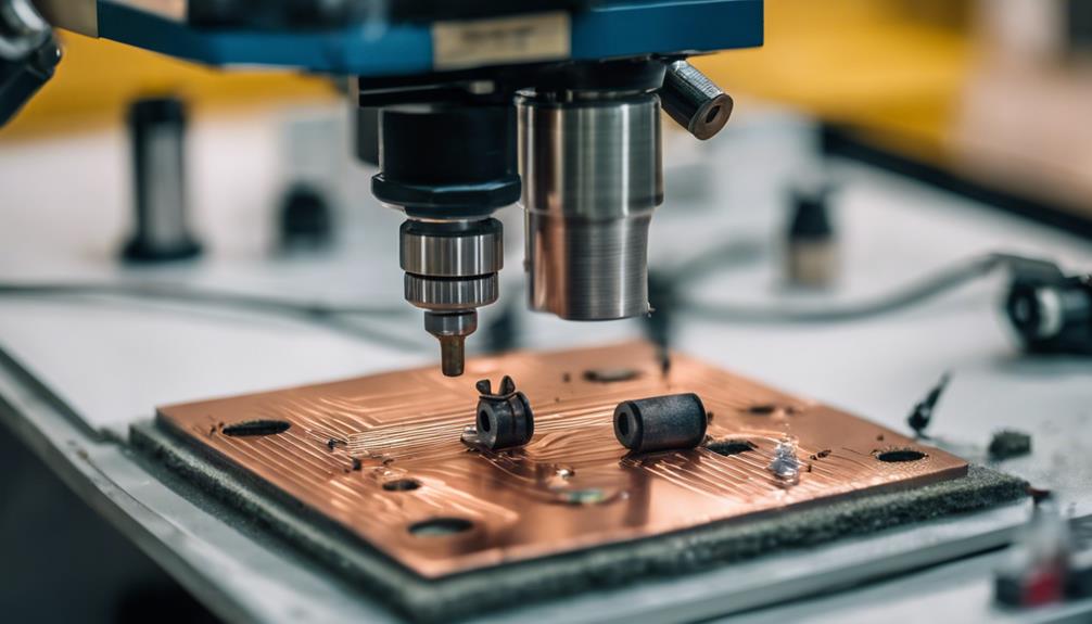
Accurate hole creation is a critical step in the PCB manufacturing process, where computer-driven machines meticulously drill precise holes for component placement, utilizing laser sensors to pinpoint drill target spots with exactitude. This guarantees that components are accurately placed, and electrical connections are secure.
| Process | Description |
|---|---|
| Drilling | Creating precise holes for component placement |
| Plating | Depositing copper in the holes for electrical connections |
| Copper Deposition | Fusing layers of the PCB together for structural integrity |
Drilling and plating are essential steps in the PCB manufacturing process to prepare the board for component assembly and functionality. The plating process involves depositing copper in the holes to ensure electrical connections. This copper deposition also helps fuse the layers of the PCB together, providing structural integrity. The combination of precise drilling and plating guarantees that the PCB is ready for component placement, ultimately leading to a functional and reliable printed circuit board.
Applying Solder Mask and Silk Screen
In the PCB prototype manufacturing process, the application of solder mask and silk screen is a critical step that guarantees the reliability and readability of the printed circuit board.
The solder mask application involves the selective coating of the PCB surface to protect copper traces and prevent solder bridges during assembly.
Next, we will explore the precise processes of solder mask application and screen printing, which are essential for producing high-quality PCB prototypes.
Solder Mask Application
Applying a solder mask and silk screen to a PCB prototype is a critical step in the manufacturing process, as it not only safeguards the board from environmental factors but also facilitates the installation of components and guarantees the overall functionality of the final product.
The solder mask application process involves applying a layer of protective coating to the PCB surface to prevent solder bridges and short circuits. This layer is typically green in color, but can also be customized to meet specific design requirements.
Here are three key aspects of solder mask application:
- Environmental protection: The solder mask protects the PCB from environmental factors such as dust and moisture, ensuring reliable operation.
- Precision application: The solder mask must be applied evenly and uniformly to prevent solder bridges and short circuits.
- Aesthetics and functionality: Silk screen printing is used to add component labels, logos, and other important information to the PCB surface, enhancing the overall appearance and functionality of the final product.
Screen Printing Process
Through the screen printing process, a precise and controlled method is employed to apply solder mask and silk screen legends onto the PCB surface, securing a high-quality finish. This process is an essential step in PCB manufacturing, as it provides a protective layer to the copper traces and conveys important information to the user.
| Screen Printing Process | Description |
|---|---|
| Stencil Preparation | A precise stencil is created with the solder mask or silk screen design |
| Solder Mask Application | Solder mask is applied through the stencil onto the PCB surface |
| Silk Screen Legend Application | Ink is applied through the stencil to create silk screen legends |
| Curing Process | The applied solder mask and silk screen legends are cured in an oven |
| Quality Control | The PCB is inspected for any defects or imperfections |
The screen printing process ensures accurate application of solder mask and silk screen details for a professional finish. The precision of this process is critical, as it directly impacts the overall quality of the PCB. By employing a professional screen printing process, PCB manufacturers can guarantee a high-reliability product that meets the demands of modern electronics.
Surface Finishing and Profiling
Surface finishing, a critical step in PCB manufacturing, plays an essential role in enhancing the functionality and longevity of printed circuit boards by protecting copper traces from environmental factors and ensuring reliable solderability. This process involves applying a thin layer of material to the surface of the PCB, which shields the copper traces from corrosion and oxidation.
Here are three essential aspects of surface finishing:
- Surface Finish Options: Immersion Silver and Immersion Gold are two popular surface finish options, each suited for different applications. Immersion Silver provides a cost-effective solution, while Immersion Gold offers superior solderability and corrosion resistance.
- Improved Solderability: Surface finishing enhances the solderability of the PCB, ensuring reliable connections and top-notch performance.
- Environmental Resistance: The surface finish protects the copper traces from environmental factors, such as moisture, humidity, and contaminants, thereby extending the lifespan of the PCB.
In addition to surface finishing, profiling involves cutting the PCB into its final shape and size, ensuring seamless integration into electronic devices. By combining these two processes, manufacturers can produce high-quality PCBs with enhanced functionality and reliability.
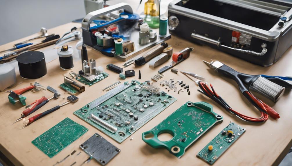
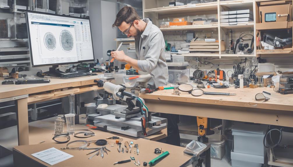
The PCB Assembly Process
Following the successful completion of surface finishing and profiling, the printed circuit board (PCB) then undergoes the assembly process, a vital stage where components are meticulously attached to create a functional circuit board.
The PCB assembly process involves the application of solder paste, followed by precise component placement, and reflow soldering to create permanent joints. To guarantee the quality of the assembly, inspection methods such as X-Ray, AOI, and manual checks are employed.
Through hole component insertion may require manual soldering techniques for precision. Once assembled, the PCB undergoes various testing methods, including in-circuit testing and flying probe testing, to verify its functionality. These testing methods are essential in ensuring the proper functioning of the final circuit board.
The PCB assembly process is a critical stage that demands meticulous attention to detail to secure the production of a high-quality, functional PCB. By combining precise component placement, reliable soldering, and rigorous testing, the assembly process sets the stage for a reliable and efficient PCB prototype.
Final Quality Check and Packaging
In the final quality check stage, a meticulous examination of each PCB prototype is conducted to verify its conformity to specifications, detect any defects, and guarantee peak functionality before packaging. This stage is essential in ensuring that the PCBs meet the customer's requirements and are free from defects.
During the final quality check, Automated Optical Inspection (AOI) machines are utilized to detect any defects or inaccuracies. Each PCB undergoes rigorous testing to ensure functionality and reliability before being packaged for shipping.
Here are the key aspects of the final quality check and packaging stage:
- Rigorous testing: Each PCB is thoroughly tested to ensure peak functionality and reliability.
- Quality control measures: Implemented to maintain high standards and meet customer requirements.
- Secure packaging: PCBs are packaged securely to protect them during transportation and storage, ensuring they reach customers in excellent condition.
Frequently Asked Questions
How Do You Manufacture a PCB Step by Step?
To manufacture a PCB, the process begins with designing the layout. This involves ensuring precise component placement and trace routing. Next, the inner layers are printed, copper traces are etched, and precision holes for components are drilled. After that, the solder mask is applied, and the outer layers are aligned and laminated. The completed PCB is then inspected for defects using automated optical inspection. Following the inspection, surface finish is applied, and electrical testing is conducted. It is important to verify that quality control measures are met to produce a high-quality PCB prototype.
How to Make a Prototype Pcb?
To create a prototype PCB, start by designing the layout using software like Altium, Eagle, or KiCad. Guarantee accurate design specifications and component placement.
Next, generate Gerber files and submit them to a quick-turn PCB manufacturer. The manufacturer will then image, etch, drill, and assemble the board.
What Are the 17 Common Manufacturing Processing Steps in PCB Production?
In PCB production, 17 meticulous steps play a vital role in ensuring precision and quality. The process initiates with imaging inner layers, followed by etching and drilling, solder mask application, and layer alignment.
Laminating, plating, and electroplating ensue, culminating in final quality checks. These checks involve electrical testing, visual inspections, and edge inspections to guarantee defect-free, high-reliability PCBs.
Each step is essential in producing high-quality, reliable prototypes and small-batch PCBs for diverse industries and applications.
How to Design a PCB for Beginners?
When designing a PCB for beginners, it is crucial to start by creating a precise schematic of the circuit design using software such as Altium, Eagle, or KiCad. This guarantees a solid foundation for the layout process.
Next, establish clear design rules, considering factors like board size, trace width, and materials to secure manufacturability and functionality.