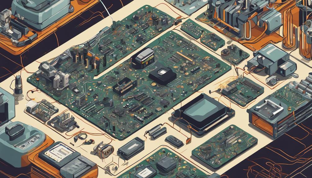
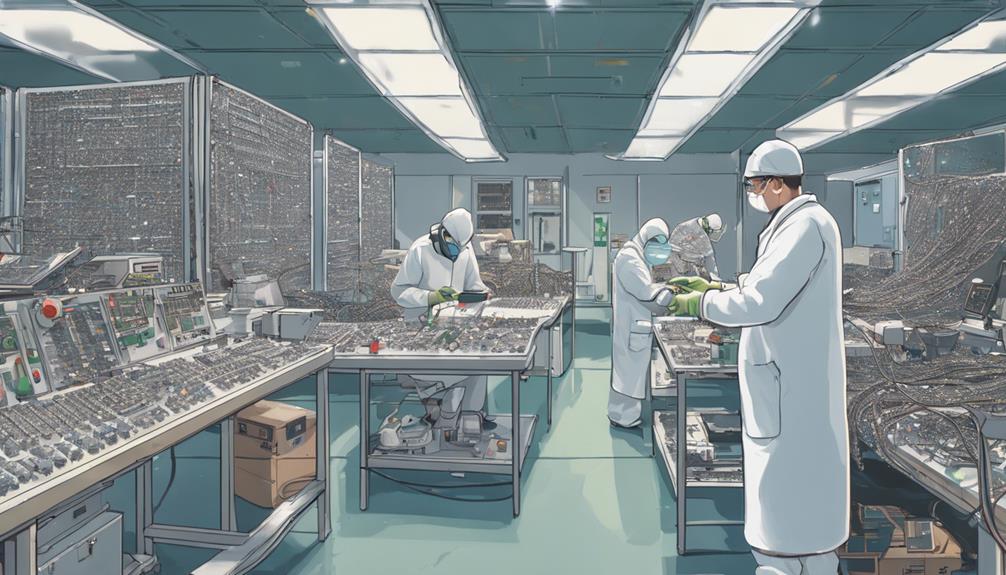
The step-by-step guide to PCB manufacturing and testing involves a meticulous process that guarantees high-quality printed circuit boards. Designing the PCB involves creating a detailed schematic, component placement, and signal routing. Inner layer processing, drilling, and deburring follow, requiring precise accuracy. Next, lamination, copper plating, and etching occur, followed by outer layer processing, solder mask application, and silkscreen printing. The final stages include electrical reliability testing, quality control, and packaging. Each step is essential for producing reliable, efficient, and high-performance PCBs. As we explore each stage, the intricacies of PCB manufacturing and testing become clear, revealing the precision and expertise involved in creating these complex electronic components.
Key Takeaways
- PCB design involves creating a detailed schematic, placing components, and considering signal routing and thermal management for optimal performance.
- Inner layer processing involves printing design files onto films, which are then stored for future reference and replication, ensuring accurate PCB functionality.
- Drilling and deburring are crucial steps that require precise drill bit selection and quality control measures to prevent accuracy degradation.
- Electroplating and etching enable intricate circuit patterns and accurate circuit patterns, respectively, which are essential for PCB functionality and reliability.
- Rigorous testing and quality control measures, including electrical reliability testing and quality control testing, ensure that PCBs meet design specifications and are reliable.
Designing the PCB
The design of a printed circuit board (PCB) begins with the creation of a detailed schematic, which serves as the foundation for the entire PCB manufacturing process. This vital step involves defining the circuit's components, interconnections, and overall architecture.
The PCB design process is a meticulous and precise endeavor, requiring careful consideration of factors such as component placement, signal routing, and thermal management.
To facilitate the design process, specialized software such as Altium and Eagle are commonly employed. These design software tools enable the creation of a precise PCB layout, ensuring that each component is accurately positioned and connected.
A critical aspect of the design process is the creation of a netlist, which assigns each pad its dedicated net for signal routing. By carefully optimizing the PCB design, manufacturers can guarantee proper component placement, interconnections, and overall functionality.
A well-designed PCB is essential for peak performance, reliability, and efficiency.
Printing the Inner Layers
Inner layer printing is a meticulous process that involves translating design files into precise films, which accurately represent the copper traces and circuits that will define the PCB's architecture. This critical step guarantees the correct layout and connections of the PCB, ultimately impacting its functionality and performance.
| Layer Type | Ink Color | Purpose |
|---|---|---|
| Inner Layer | Clear | Accurate reproduction of copper traces |
| Inner Layer | Black | Accurate reproduction of circuits |
| Reference Film | Clear | Storage for future replication |
| Reference Film | Black | Storage for future replication |
The films created during this step are stored for future reference and replication in the PCB manufacturing process. Precise printing of the inner layers is essential to safeguard the functionality and performance of the final PCB. Any inaccuracies or defects in the printing process can lead to faulty or non-functional PCBs. Hence, it is crucial to maintain high standards of quality control during the inner layer printing process to guarantee the production of reliable and efficient PCBs.
Drilling and Deburring
In the drilling and deburring stage of PCB manufacturing, the selection of drill bits and the control of hole quality are critical factors that greatly impact the overall performance of the printed circuit board.
The type of drill bit chosen can affect the accuracy of hole placement, size, and surface finish, while hole quality control measures guarantee that the drilled holes meet the required specifications.
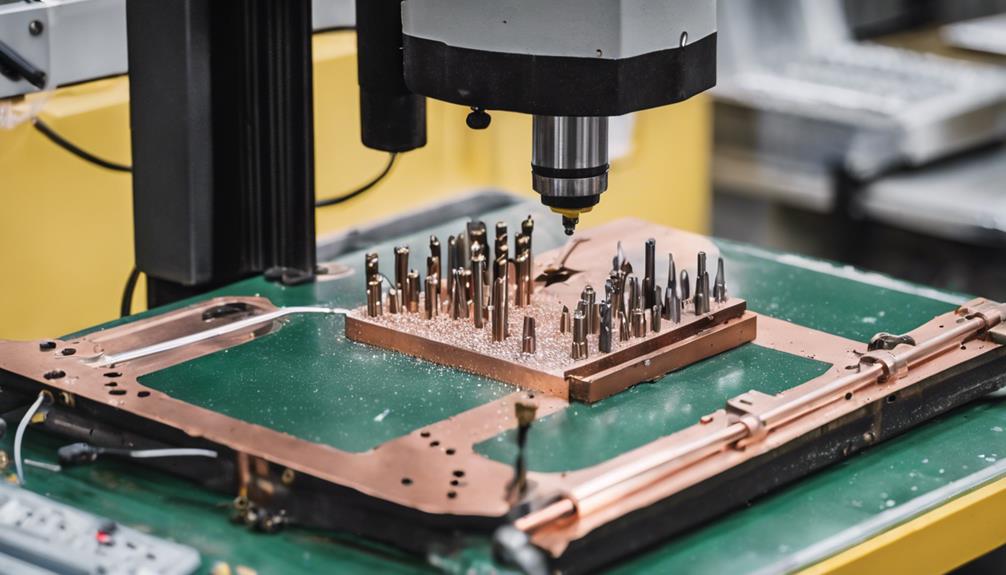
Drill Bit Selection
During the PCB manufacturing process, selecting the appropriate drill bit is vital, as it directly impacts the accuracy and quality of the final product. Solid carbide PCB drill bits are the preferred choice due to their durability and precision. These specialized drill bits are designed with a high aspect ratio to prevent burrs and guarantee clean hole walls.
| Drill Bit Characteristic | Description |
|---|---|
| Material | Solid carbide for durability and precision |
| Aspect Ratio | High to prevent burrs and guarantee clean hole walls |
| Size Range | 0.1mm to 6mm for various hole requirements |
| Flute Design | Facilitates chip removal for accuracy |
| Deburring | Essential to remove sharp edges and burrs |
The flute design of PCB drill bits is essential for chip removal during the drilling process, ensuring accuracy and precision. Additionally, deburring tools are necessary to eliminate any sharp edges or burrs that may affect the PCB's functionality. By selecting the right drill bit, manufacturers can secure high-quality holes and prevent defects in the final product.
Hole Quality Control
In order to guarantee the reliability and performance of printed circuit boards, stringent hole quality control measures are implemented to scrutinize every aspect of the drilling and deburring process. The drilling process in PCB manufacturing involves creating holes for component placement with precision, and any defects can compromise the entire board.
To secure top-notch hole quality, manufacturers must implement strict quality control measures, including:
- Monitoring drill bit wear to prevent degradation of hole accuracy
- Verifying alignment accuracy to ensure precise hole placement
- Checking hole size consistency to guarantee uniformity
Proper deburring techniques are also essential to remove sharp edges around drilled holes, preventing damage to components and ensuring smooth hole surfaces for secure component insertion.
Lamination and Pressing

In the lamination and pressing stage of PCB manufacturing, the layer stackup configuration plays a vital role in determining the final structure of the board.
The copper foil application process, which involves applying copper foils to the prepreg layers, is also an essential aspect of this stage.
Layer Stackup Configuration
What constitutes a well-designed layer stackup configuration, and how do the specific arrangements of copper layers, prepreg, and substrate materials impact the overall performance of a PCB?
A well-designed layer stackup configuration is important for achieving excellent PCB performance. It involves determining the order and arrangement of copper layers, prepreg, and substrate materials to meet specific design requirements.
The layer stackup configuration directly impacts the electrical and mechanical properties of the PCB, affecting signal integrity, impedance control, and thermal management. Different PCB designs require specific layer stackup configurations to meet performance requirements.
Proper layer stackup configuration ensures optimal signal integrity and impedance control. It enables effective thermal management and reduces the risk of overheating. A well-designed layer stackup configuration enhances the overall reliability and performance of the PCB.
In the pressing process, the carefully arranged layers are laminated together to form a single, cohesive unit. This process requires precision and attention to detail to ensure the layers are properly aligned and bonded.
A well-designed layer stackup configuration is essential for producing high-quality PCBs that meet the required performance standards.
Copper Foil Application
How does the precise application of copper foil, involving lamination and pressing, impact the formation of reliable conductive pathways in a PCB? The answer lies in the importance of the bond between the copper foil and the substrate. Copper foil application involves laminating copper sheets to the substrate using heat and pressure, ensuring a strong bond for efficient conductivity. Pressing the copper foil onto the substrate is vital for creating the conductive pathways in the PCB.
| Parameter | Best Value | Impact on Conductivity |
|---|---|---|
| Lamination Temperature | 180°C – 200°C | Ensures robust substrate bonding |
| Pressing Pressure | 100 – 150 psi | Prevents delamination and guarantees conductivity |
| Copper Foil Thickness | 18 μm – 35 μm | Affects signal integrity and conductivity |
| Substrate Material | FR4, FR5, or High-Tg | Influences thermal resistance and durability |
| Bonding Time | 30 minutes – 1 hour | Affects substrate bonding strength |
Proper lamination and pressing techniques prevent delamination and ensure the integrity of the copper traces. The quality of copper foil application significantly impacts the overall performance and reliability of the PCB. By controlling these parameters, manufacturers can guarantee the formation of reliable conductive pathways, ultimately leading to high-quality PCBs.
Copper Plating and Etching
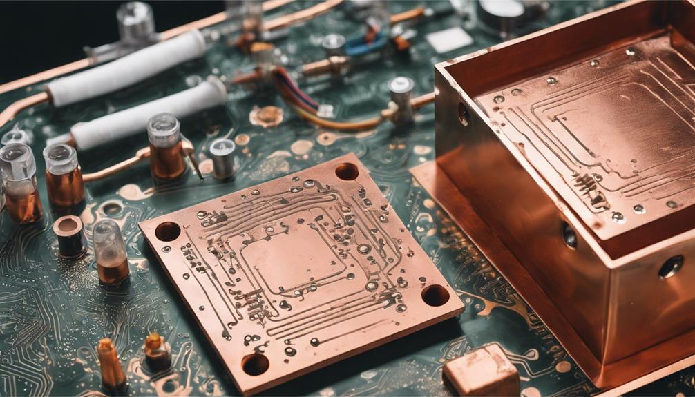
During the PCB manufacturing process, a critical step involves depositing a thin layer of copper onto the substrate through electroplating or electroless plating, a process known as copper plating. This process helps create electrical connections and pathways on the PCB. The thin layer of copper is essential for the functionality and reliability of the PCB.
Copper plating enables the creation of intricate circuit patterns on the PCB surface.
Chemical etching is used to remove excess copper, leaving behind the desired copper traces.
Precise etching techniques are vital to guarantee accurate circuit patterns on the PCB.
Copper plating and etching techniques are critical components of the PCB manufacturing process. The thin layer of copper deposited during plating allows for the creation of complex circuit patterns, while chemical etching ensures that only the desired copper traces remain. The precision of these techniques directly impacts the functionality and reliability of the final PCB product.
Outer Layer Imaging

Outer layer imaging, a critical stage in the PCB manufacturing process, involves the precise transfer of the PCB design onto the outer copper layers, leveraging films created during inner layer imaging to guarantee accurate replication of circuitry patterns.
This process is essential for ensuring the fidelity of the PCB's electrical connections. During outer layer imaging, UV light exposure is utilized to define the traces and pads on the outer layers. The films created during inner layer imaging serve as a template, allowing for precise alignment of the outer layer components.
Proper alignment is necessary to ensure accurate placement of components, as misalignment can lead to faulty PCBs. By accurately transferring the PCB design onto the outer copper layers, outer layer imaging plays a pivotal role in ensuring the reliability and functionality of the final PCB product.
Through precise UV light exposure and alignment, outer layer imaging enables the creation of high-quality PCBs that meet the demands of modern electronic devices.
Solder Mask Application
With the precise transfer of the PCB design onto the outer copper layers complete, attention turns to the application of solder mask, a critical process that restricts solder flow to specific areas, ensuring reliable connections and preventing short circuits. This process is vital for PCB reliability, as it prevents oxidation and environmental damage to the copper traces underneath.
The solder mask application process involves various methods, including Epoxy Liquid, Liquid Photo Imageable, and Dry Film Photo Imageable, chosen based on design requirements.
Inkjet printing technology offers improved resolution and selective thickness control for precise application of solder mask. The curing process, which involves high-temperature treatment, ensures good adhesion of the solder mask to the PCB surface, enhancing its durability and protection.
- Solder mask application methods include Epoxy Liquid, Liquid Photo Imageable, and Dry Film Photo Imageable.
- Inkjet printing technology provides improved resolution and selective thickness control.
- Curing the solder mask at high temperatures ensures good adhesion to the PCB surface.
Silkscreen Printing and Finishing

Precision is paramount in silkscreen printing, a critical process that adds important information to the PCB, facilitating effortless component identification and assembly. This process is essential for guaranteeing accurate component placement during PCB assembly and repair. The silkscreen layer is applied after solder mask application to ensure clear visibility. The use of a white ink layer provides contrast against the PCB's base color, making it easier to read.
Silkscreen printing is responsible for adding component designators, logos, and other identification information to the PCB. This information is essential for identifying components and ensuring proper assembly.
| Silkscreen Printing Benefits | Description | Importance |
|---|---|---|
| Component Identification | Enables easy identification of components | Critical for assembly and repair |
| Accurate Placement | Facilitates precise component placement | Ensures proper assembly and functionality |
| Visual Contrast | Provides clear visibility against PCB's base color | Enhances readability |
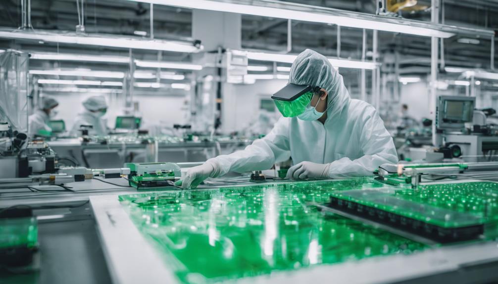
Electrical Reliability Testing
Electrical reliability testing involves a range of assessments to guarantee PCBs meet performance standards. Among these, Voltage Stress Testing and Environmental Simulation are vital components.
Voltage Stress Testing subjects the PCB to controlled voltage fluctuations to identify potential weaknesses. Environmental Simulation replicates real-world operating conditions to gauge the board's resilience.
Voltage Stress Testing
Voltage stress testing is an essential component of electrical reliability testing. It simulates extreme operating conditions to evaluate a PCB's ability to withstand high voltage levels and identify potential weaknesses in insulation, components, and overall performance.
During voltage stress testing, PCBs are subjected to high voltage levels to assess their reliability and durability under extreme conditions. This testing is vital for ensuring the reliability and durability of PCBs in real-world operating conditions.
This process helps in identifying potential short circuits, breakdowns, or insulation failures in PCBs under extreme voltage conditions. It also provides valuable data for improving PCB design, manufacturing processes, and overall product quality.
Ultimately, voltage stress testing enhances the overall reliability and performance of PCBs in various applications.
Environmental Simulation
Beyond voltage stress testing, which evaluates a PCB's ability to withstand high voltage levels, environmental simulation testing is employed to assess a PCB's performance and reliability under diverse, harsh environmental conditions. This type of testing is pivotal in PCB production, as it helps identify potential weaknesses in the design and manufacturing process.
Environmental simulation testing involves subjecting PCBs to extreme conditions such as temperature, humidity, and vibration, mimicking real-world scenarios. Accelerated aging tests are conducted to predict the PCB's lifespan and performance over time, guaranteeing that the final product meets industry standards.
Compliance with standards like IPC-9592 ensures that PCBs meet reliability requirements. By simulating environmental stressors, manufacturers can identify and address potential faults, ensuring that the final product is reliable and efficient.
Environmental testing is a critical step in the PCB manufacturing process, allowing manufacturers to refine their designs and production methods to produce high-quality, reliable PCBs.
Final Inspection and Packaging
During the final stage of PCB manufacturing, a meticulous inspection is conducted to guarantee that the printed circuit boards meet the required standards and customer specifications. This final inspection involves visual checks for defects, solder mask coverage, and component placements. Any discrepancies found during this process can lead to rework or rejection of the PCB.
- Final inspection ensures compliance with industry standards and customer specifications
- Visual checks are conducted for defects, solder mask coverage, and component placements
- Any discrepancies can lead to rework or rejection of the PCB
Once the PCBs have passed the final inspection, they are packaged with protective materials to prevent damage during shipping. Proper documentation and certificates are included in the packaging for traceability and compliance. This secures that the PCBs are delivered to customers in pristine condition, meeting their specifications and requirements.
The final inspection and packaging stage is pivotal in guaranteeing the quality and reliability of the printed circuit boards.
What are the Testing Methods Used in PCB Manufacturing?
When it comes to fabricating printed circuit board essentials, there are various testing methods used in PCB manufacturing to ensure quality and reliability. These methods include visual inspection, automated optical inspection, flying probe testing, and in-circuit testing. Each method plays a crucial role in detecting any potential issues and defects in the manufactured PCBs.
Quality Control and Shipping
In order to guarantee the highest level of quality and reliability, PCB manufacturers employ a range of testing methodologies, including in-circuit testing, automated optical inspection, and X-ray inspection, to verify the functionality and performance of printed circuit boards. Each PCB undergoes rigorous testing to guarantee functionality, reliability, and adherence to design specifications. Flying probe tests and burn-in tests are common methods used to verify the quality and performance of PCBs.
| Testing Method | Description | Purpose |
|---|---|---|
| In-Circuit Testing | Tests individual components on the PCB | Verify component functionality |
| Automated Optical Inspection | Inspects the PCB for defects and faults | Detects visual defects |
| X-Ray Inspection | Inspects the internal layers of the PCB | Verifies internal connections |
Proper packaging and shipping procedures are essential to protect PCBs during transportation and delivery to customers. Certificates and documentation are vital for verifying the quality of PCBs and providing necessary information to customers. By implementing stringent quality control measures, PCB manufacturers can ensure the delivery of high-quality products that meet customer requirements.
Frequently Asked Questions
How Do You Manufacture a PCB Step by Step?
To manufacture a PCB, the process begins by preparing the raw materials. This includes acquiring copper-clad laminate and photoresist.
Next, the inner layers are created through various steps such as imaging, etching, and lamination.
Drilling holes for through-hole components comes next, followed by processes like copper plating and solder mask application.
Surface finishing options, like immersion silver or gold, are then applied for protection and functionality.
What Are the Steps for PCB Testing?
When undertaking PCB testing, a multi-faceted approach is essential. Initially, in-circuit testing is employed to detect shorts and opens, ensuring proper circuit functionality.
Next, automated optical inspection is utilized to identify defects such as missing components or misalignments.
Flying probe testing is then conducted to assess connectivity and functionality without a test fixture.
What Are the 17 Common Manufacturing Processing Steps in PCB Production?
In PCB production, 17 essential manufacturing steps are vital for creating reliable printed circuit boards. These steps include:
- Imaging
- Etching
- Drilling
- Solder mask application
- Layer alignment
- Lamination
- Plating
- Quality checks
Each step guarantees precise layer alignment, defect-free drilling, and adequate plating thickness. Stringent quality control measures, including automated optical inspection, ensure high-quality PCBs for diverse electronic applications.
What Are the 7 Types of PCB Testing Methods?
In the domain of printed circuit board (PCB) testing, seven distinct methods are employed to guarantee the reliability and quality of PCBs. These methods include In-circuit Test, Automated Optical Inspection, Flying Probe Test, Burn-In Test, and X-Ray Inspection, each serving a unique purpose in detecting defects and anomalies.