Mastering the PCB manufacturing process requires a deliberate and meticulous approach that encompasses a range of critical considerations, from strategically selecting materials and optimizing design for manufacturability to implementing efficient manufacturing techniques and ensuring adherence to industry standards. Effective PCB manufacturing involves choosing the right materials, designing for manufacturability, streamlining production workflows, and conducting rigorous quality control measures. Additionally, ensuring compliance with industry standards, sourcing high-quality components, and streamlining the PCB assembly process are essential for producing reliable and high-quality PCBs. By addressing these essential factors, manufacturers can optimize their PCB manufacturing process for improved efficiency, quality, and reliability. Further exploration of these critical considerations will reveal the nuances of mastering the PCB manufacturing process.
Key Takeaways
- Optimize PCB material selection considering signal integrity, thermal dissipation, and reliability to ensure high-quality boards.
- Design for manufacturability by following DFM guidelines and collaborating with manufacturers to enhance fabrication and assembly processes.
- Implement efficient manufacturing techniques, such as automated pick-and-place machines and advanced inspection methods, to streamline production.
- Ensure rigorous quality control throughout the production process, adhering to industry standards like IPC-A-610 and ISO 9001.
- Verify component authenticity and reliability by maintaining accurate inventory records and utilizing approved vendor lists to prevent counterfeit components.
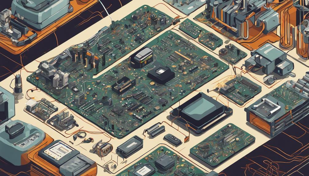
Selecting the Right PCB Materials
When designing a printed circuit board (PCB), selecting the right material is an important decision that can significantly impact the board's performance, reliability, and cost.
The choice of material affects the circuit's signal integrity, thermal dissipation, and overall reliability. Factors such as dielectric constant, thermal conductivity, and cost must be carefully considered.
Popular PCB materials include FR-4, high-frequency materials like Rogers, and flexible materials like polyimide. Advanced materials like ceramic substrates offer excellent thermal management and high-frequency performance.
Understanding material properties is essential for optimizing signal integrity, thermal dissipation, and reliability. It is essential to consult with PCB manufacturers for recommendations on materials based on specific design requirements.
By selecting the right material, designers can ensure their electronic components operate efficiently and effectively, streamlining the manufacturing process and reducing testing time.
Optimizing PCB Design for Manufacturability
Optimizing PCB design for manufacturability is essential to guarantee that the final product meets performance and reliability requirements.
This involves considering key design parameters, such as component placement and PCB material selection, to facilitate efficient fabrication and assembly processes.
Design for Fabrication
Designing for fabrication is a pivotal step in the PCB manufacturing process, as it lays the foundation for efficient production by carefully considering factors such as component placement, trace routing, and layer stackup. By optimizing PCB layouts, designers can minimize production errors, reduce costs, and improve overall quality. Implementing DFM guidelines and collaborating with manufacturers early in the design phase helps streamline fabrication and assembly processes.
| Design Aspect | Impact on Manufacturability | Optimization Strategy |
|---|---|---|
| Component Placement | Improper placement increases production errors | Follow DFM guidelines for best placement |
| Trace Routing | Inefficient routing increases production time | Enhance routing using PCB design software |
| Layer Stackup | Inadequate layer stackup reduces yields | Collaborate with manufacturers to enhance layer stackup |
Component Placement Strategies
Effective component placement is critical in PCB design, as it directly influences the manufacturability, reliability, and overall performance of the final product. A well-planned component placement strategy can greatly impact the PCB manufacturing process, ensuring excellent performance, and reducing production costs.
To achieve reliable PCB assembly, consider the following component placement strategies:
- Group related components together to minimize trace lengths and improve signal integrity.
- Place high-speed components closer together to reduce signal delays and impedance mismatches.
- Consider manufacturability factors such as assembly process efficiency and accessibility when positioning components on the board.
- Utilize design software tools to simulate and analyze component placement for excellent performance and ease of manufacturing.
PCB Material Selection
Selecting the most suitable PCB material is a critical aspect of optimizing PCB design for manufacturability. It directly influences the performance, reliability, and overall cost of the final product. The choice of material can have a major impact on the thermal conductivity, dielectric constant, and signal integrity of the PCB. Common materials like FR-4, polyimide, and Rogers are popular for their unique properties and cost-effectiveness.
However, high-frequency applications may require specialized materials like PTFE to achieve desired signal integrity and performance. When choosing a PCB material, it is essential to take into account factors such as thermal conductivity, dielectric constant, and cost.
Collaboration with PCB manufacturers and material suppliers can provide valuable insights into selecting the most suitable material for specific design requirements. Understanding the properties and limitations of different PCB materials enables informed decisions for efficient manufacturing processes.
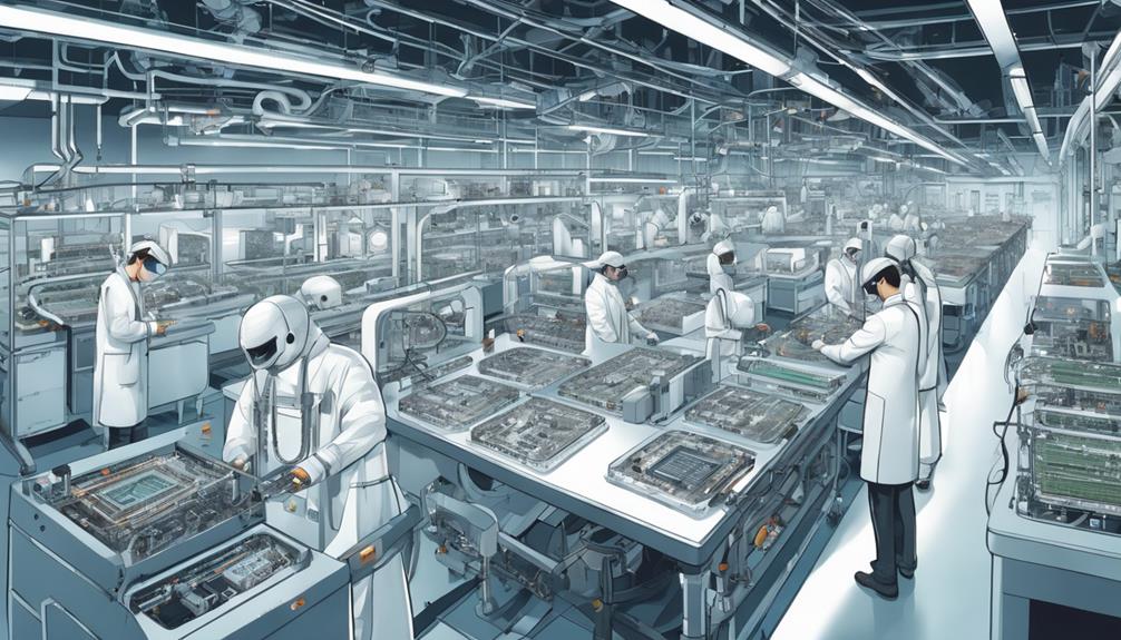
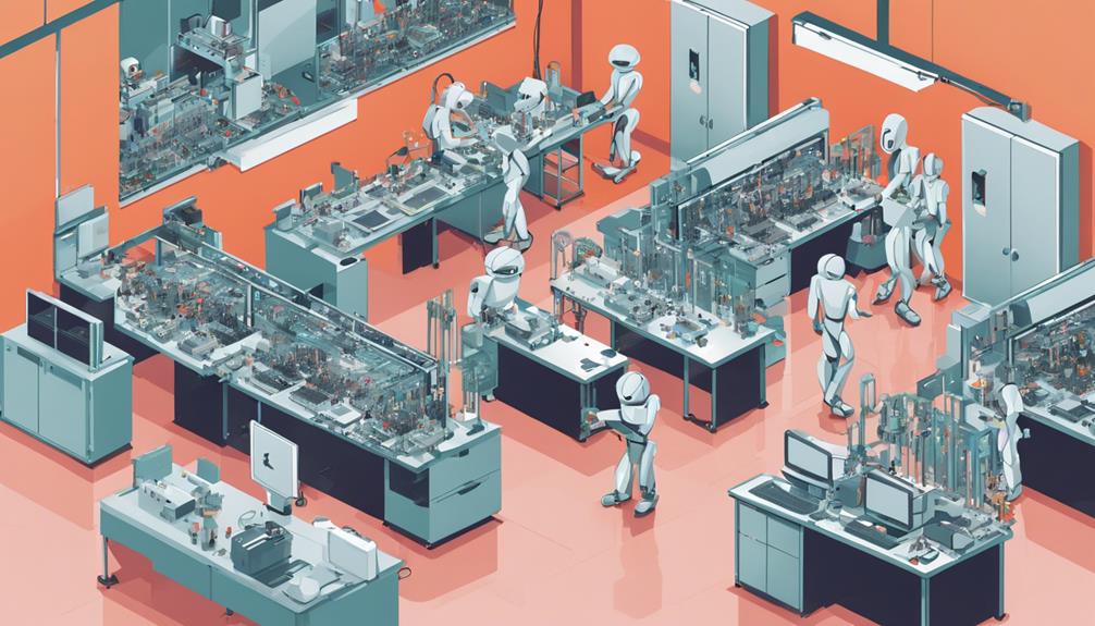
Implementing Efficient Manufacturing Techniques
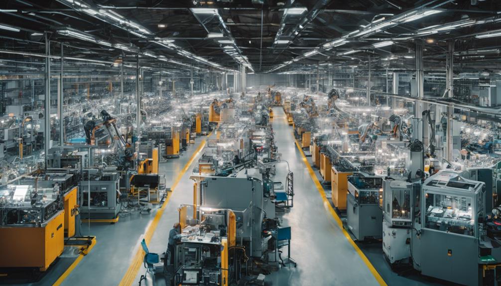
Implementing efficient manufacturing techniques is vital for minimizing production time and costs while maintaining high-quality PCBs.
To achieve this, manufacturers can adopt streamlined production workflows and lean manufacturing strategies that eliminate waste and maximize productivity.
Streamlined Production Workflow
By integrating advanced manufacturing techniques, such as automated pick-and-place machines and advanced inspection methods, PCB manufacturers can greatly enhance the efficiency and quality of their production workflow.
This streamlined approach enables manufacturers to optimize their PCB manufacturing process, resulting in improved product quality and reduced production time.
To achieve a streamlined production workflow, manufacturers can implement the following techniques:
- Employ automated pick-and-place machines to enhance component placement efficiency
- Utilize advanced inspection methods, such as AOI and electrical testing, to maintain high manufacturing standards
- Leverage CNC technology to enable precise and accurate PCB fabrication
- Implement wave soldering and reflow soldering techniques to optimize the soldering process and guarantee consistent, reliable solder joints
Lean Manufacturing Strategies
To optimize PCB manufacturing efficiency, manufacturers can adopt lean manufacturing strategies that eliminate waste, optimize processes, and improve overall production quality. By implementing lean principles, PCB manufacturers can streamline their production workflow, reduce lead times, and enhance overall quality.
Techniques such as 5S methodology, value stream mapping, and Kanban systems are commonly used in lean manufacturing for PCB production. These strategies help eliminate waste, optimize processes, and improve efficiency, resulting in cost savings, increased productivity, and improved customer satisfaction.
Continuous improvement and employee involvement are key aspects of successfully implementing lean manufacturing strategies in PCB production. By adopting lean practices, PCB manufacturers can reduce lead times, minimize inventory, and enhance overall production quality. This, in turn, leads to cost savings, increased productivity, and improved customer satisfaction.
Conducting Thorough Quality Control Measures
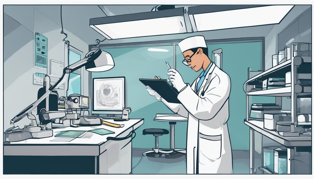
To guarantee the reliability and performance of printed circuit boards (PCBs), manufacturers must conduct rigorous quality control measures throughout the production process. This involves adhering to industry standards such as IPC-A-610 and ISO 9001, making sure that PCBs meet the required quality standards.
Effective quality control measures include:
- Implementing inspection methods such as visual, AOI, and electrical testing to identify defects and maintain PCB reliability
- Conducting reliability testing techniques like stress tests and X-ray technology to pinpoint potential issues early on
- Following systematic approaches to quality control to uphold the highest standards in PCB manufacturing
- Meeting quality standards to secure PCB reliability over its lifespan
Ensuring Adherence to Industry Standards

Manufacturers must adhere to industry standards, such as IPC-A-600 and IPC-6012, to guarantee the quality and reliability of printed circuit boards, as non-compliance can result in defects, inconsistencies, and ultimately, product failure. Adherence to industry standards ensures that circuit boards meet the required quality, functionality, and performance criteria. Compliance with standards aids in reducing defects, enhancing consistency, and improving overall product quality.
| Industry Standards | PCB Design Process | Compliance Benefits |
|---|---|---|
| IPC-A-600 | Material selection | Reduced defects |
| IPC-6012 | Fabrication processes | Enhanced consistency |
| IPC-6013 | Testing procedures | Improved product quality |
| J-STD-001 | PCB fabrication | Increased reliability |
| ISO 9001 | Certification | Customer satisfaction |
Effective Component Sourcing and Management
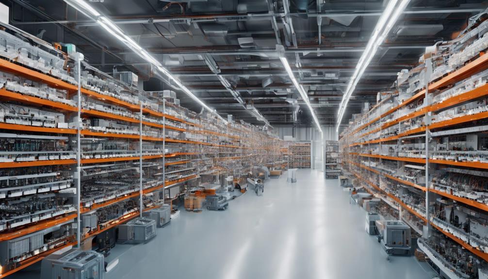
Effective component sourcing and management are critical aspects of PCB manufacturing, as they directly impact production efficiency, cost control, and ultimately, the quality of the final product. In the production of high-quality circuit boards, reliable component sourcing and management are essential to guarantee the timely delivery of quality components.
To achieve efficient component sourcing and management, the following strategies are essential:
Identify reliable suppliers with quality products and timely delivery to secure a steady supply of components.
Maintain accurate inventory records and track lead times for reordering to prevent stockouts and overstocking.
Utilize approved vendor lists to validate the authenticity and reliability of sourced components.
Implement a robust component verification process to thwart counterfeit components from entering the production line.
Streamlining the PCB Assembly Process
Following the careful selection and management of high-quality components, the PCB assembly process is where these components come together to form a functional circuit board, and it is here that efficient production processes and quality control measures are essential.
To streamline the PCB assembly process, it is vital to utilize automated pick-and-place machines for efficient and accurate component placement. This ensures that components are precisely placed, reducing the risk of human error and defects. Advanced soldering techniques, such as wave soldering and reflow soldering, should also be implemented to guarantee reliable connections.
Additionally, thorough inspection and testing of assembled PCBs are critical to ensure quality and functionality. AOI and electrical testing methods can be employed to detect defects and ensure compliance with quality standards.
Frequently Asked Questions
What Are the 17 Common Manufacturing Processing Steps in PCB Production?
Like a masterful conductor leading an orchestra, the PCB manufacturing process harmoniously orchestrates 17 distinct steps to produce a precision-crafted board. From laminate cutting to solder mask application, each step is meticulously carried out to guarantee a flawless final product.
The 17 steps are:
- Laminate cutting
- Drilling
- Deburring
- Plating
- Etching
- Stripping
- Imaging
- Developing
- Etch resist applying
- Tin plating
- Solder mask application
- Surface finishing
- Component mounting
- Inspection
- Testing.
How Do You Manufacture a PCB Step by Step?
To manufacture a PCB, the process begins with creating a blueprint and transforming it into a film.
Next, the inner layers are printed and synchronized, followed by drilling precise holes and plating for copper deposition.
Outer layer imaging and optical inspection are then conducted to guarantee quality control.
The next steps involve layering up and bonding the outer layers to the substrate.
What Is the Most Essential Step in PCB Designing?
The most essential step in PCB designing is creating a clear and accurate schematic layout.
This foundational step sets the tone for the entire design process, influencing component placement and routing decisions.
A well-organized schematic guarantees accurate representation of components and connections, minimizing errors and streamlining the design process.
What Are the Golden Rules of PCB Design?
Did you know that 80% of PCB design errors can be attributed to poor design practices? To avoid such pitfalls, adhering to the golden rules of PCB design is essential.
These rules encompass a set of guidelines that guarantee excellent PCB performance, reliability, and manufacturability. Key principles include minimizing signal path lengths, optimizing component placement, and maintaining signal integrity through careful trace routing and layer stacking.