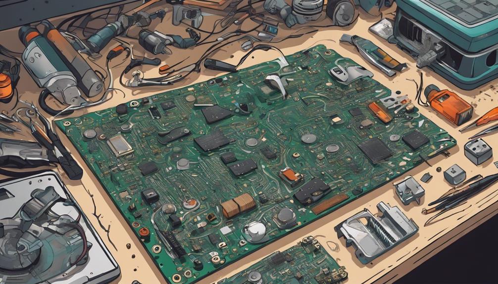
PCB manufacturers rely on accurate and efficient defect detection methods to guarantee the production of high-quality printed circuit boards. Three essential defect detection methods exist: automated defect detection, visual inspection techniques, and advanced defect analysis tools. Automated methods utilize cameras and algorithms to detect subtle defects, reducing human error and increasing production efficiency. Visual inspection techniques, widely used by manufacturers, detect missing components and soldering issues. Advanced analysis tools enhance defect detection accuracy and streamline quality control. By combining these methods, manufacturers can achieve peak defect detection and improve overall product quality, and exploring each method in more detail can reveal further benefits and applications.
Key Takeaways
- Automated Optical Inspection (AOI) systems enhance defect detection accuracy by minimizing human error and detecting subtle defects.
- Visual inspection techniques are cost-effective, but augmenting with AOI systems ensures reliable and efficient defect detection.
- Advanced defect analysis tools, such as AOI systems, detect subtle defects that evade human inspectors, improving accuracy by up to 5.6% for specific defects.
- Implementing AOI systems can enhance accuracy, reduce parameters by 35%, and optimize industrial automation for quality control.
- Effective defect detection methods, including AOI and visual inspection, ensure only defect-free PCBs reach the production line, improving overall product quality.
Automated Defect Detection Methods
Implementing automated defect detection methods, such as AOI systems, greatly enhances the accuracy of identifying PCB defects, thereby reducing the likelihood of human error and increasing production efficiency.
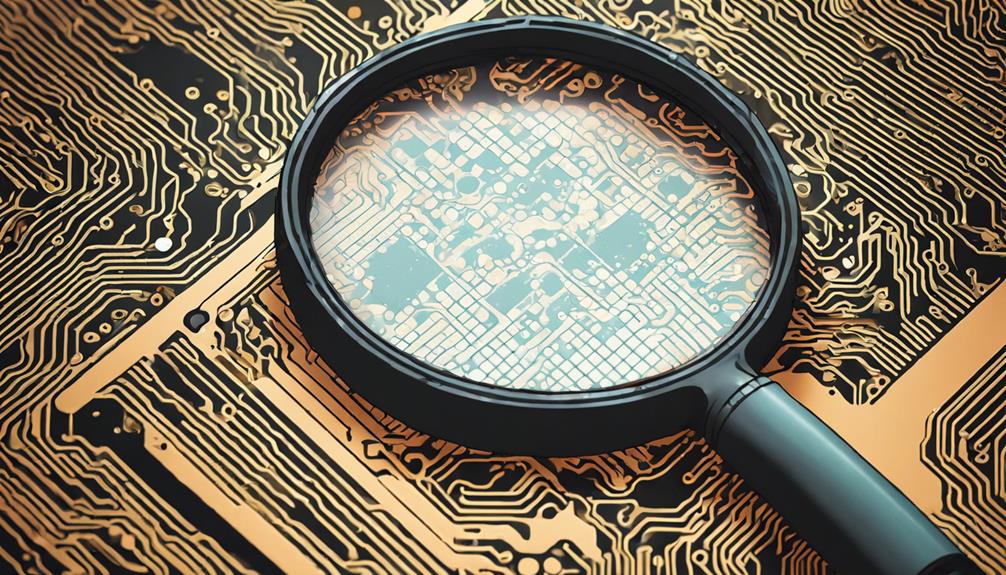
AOI systems utilize cameras and algorithms to inspect PCBs for defects, including missing components or soldering issues. This automated approach minimizes the risk of human error, ensuring that defective products do not reach the market.
By leveraging advanced image processing techniques, AOI systems can detect even the most subtle manufacturing defects, ensuring that only high-quality PCBs are produced. As a result, electronic products manufactured using these automated defect detection methods are more reliable, reducing the risk of faulty units and enhancing overall quality control.
Visual Inspection Techniques
Among the various defect detection methods employed by PCB manufacturers, visual inspection techniques remain a widely used approach for identifying defects in printed circuit boards. These techniques involve a thorough visual examination of the PCB to detect defects such as missing components, soldering issues, and PCB traces.
While visual inspection is a cost-effective method, it may miss subtle defects, highlighting the importance of augmenting human inspection with automated optical inspection (AOI) systems. AOI systems enhance the accuracy of visual inspections, offering high accuracy in defect detection. These systems can detect defects that may be overlooked by human inspectors, guaranteeing that only defect-free PCBs reach the production line.
However, implementing AOI systems can be expensive. By combining visual inspection with AOI, PCB manufacturers can ensure reliable and efficient defect detection, resulting in high-quality electronic components and reduced PCB defect detection rates.
Advanced Defect Analysis Tools

Beyond visual inspection, advanced defect analysis tools have emerged as an essential component of quality control in PCB manufacturing, capable of detecting subtle defects that may evade human inspectors. Automated Optical Inspection (AOI) systems are a prime example of advanced defect analysis tools, offering detailed inspection capabilities for identifying defects such as open circuits and missing components. These systems avoid mechanical damage to PCBs and scale easily for high-volume production.
| Defect Type | AOI System Capability | Accuracy Improvement |
|---|---|---|
| Open circuits | Detection of subtle cracks | 4.2% |
| Missing components | Identification of component absence | 3.8% |
| Surface defects | Detection of scratches and corrosion | 5.1% |
| Misaligned components | Detection of component misalignment | 4.5% |
| Short circuits | Detection of unintended connections | 5.6% |
The implementation of AOI tools can improve overall accuracy by up to 5.6% for specific defects. Compared to traditional methods, AOI systems require 35% fewer parameters, reducing complexity and cost. By leveraging advanced defect analysis tools like AOI systems, PCB manufacturers can enhance defect detection accuracy, streamline quality control, and optimize industrial automation.
Frequently Asked Questions
How Do You Find Defects in Pcb?
'What lies beneath the surface of a PCB is often shrouded in mystery, but it's a puzzle that must be solved to guarantee quality.
To find defects in PCBs, a multi-faceted approach is crucial. Visual inspection and automated optical inspection (AOI) provide a first line of defense, while X-ray inspection and in-circuit testing (ICT) explore deeper to detect internal and electrical faults.
Functional testing then verifies overall performance, establishing a thorough defect detection strategy.'
What Are Defect Detection Techniques?
Defect detection techniques are essential in ensuring the quality of printed circuit boards (PCBs).
Various methods are employed to identify defects, including:
- Visual inspection
- Automated optical inspection (AOI)
- X-ray inspection
- In-circuit testing (ICT)
- Functional testing
These techniques offer distinct advantages and limitations, necessitating a multi-faceted approach to defect detection.
How Do You Find Faulty Components on a Pcb?
To identify faulty components on a printed circuit board (PCB), manufacturers employ various defect detection methods. Automated optical inspection (AOI) systems utilize cameras and algorithms to detect visual defects, such as missing or misaligned components.
X-ray inspection is also used to non-invasively detect internal faults.
In-circuit testing (ICT) and functional testing further verify the electrical and functional integrity of components, enabling effective fault detection and isolation.
What Is the Most Versatile Tool to Troubleshoot a Pcb?
When troubleshooting a PCB, the most versatile tool is the oscilloscope. This device provides real-time visualization of signal behavior, enabling the identification of abnormalities.
By measuring voltage waveforms, frequency, and signal timing, oscilloscopes help locate issues such as signal distortions, noise, or improper voltage levels.
With various probe types and advanced features, oscilloscopes offer unparalleled diagnostic capabilities, making them an essential tool for PCB troubleshooting.