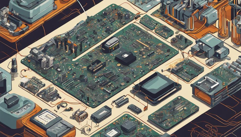
Fabricating a printed circuit board (PCB) requires attention to detail and adherence to specific guidelines to guarantee high-quality and reliable boards. To achieve this, it is vital to perform design for manufacturability checks, select high-quality materials, and handle sensitive components with care. Precision drilling, skillful soldering, and regular quality control measures are also key. Moreover, adhering to industry standards ensures uniformity in fabrication processes and materials. By following these essential tips, manufacturers can ensure the production of high-quality PCBs. To guarantee excellent PCB fabrication, it is critical to implement these guidelines meticulously, and a thorough understanding of each can make all the difference.
Key Takeaways
- Optimize PCB design for efficient production using Design for Manufacturability Checks.
- Select base materials and surface finishes that meet performance, reliability, and durability requirements.
- Handle sensitive components with care to prevent contamination and damage, using ESD protection measures.
- Employ precision drilling and skillful soldering techniques, with regular quality control through visual inspections and electrical testing.
- Adhere to industry standards like IPC-A-600 and IPC-6012 to ensure quality and reliability in fabrication processes and materials.
Design for Manufacturability Checks
Regularly, design teams prioritize Design for Manufacturability (DFM) checks to make sure that their printed circuit board (PCB) design aligns with manufacturing capabilities and standards. This critical step guarantees that the PCB design is optimized for efficient production, reducing costs and potential errors.
Key factors in DFM checks include component placement, routing, spacing, and trace width considerations. By conducting DFM checks early in the design process, designers can prevent costly redesigns and delays in production. This proactive approach enables designers to identify and address potential manufacturing issues before they become major problems.
Effective DFM checks facilitate collaboration between designers and manufacturers, ensuring that the PCB design meets manufacturing capabilities and standards. By integrating DFM checks into the early design process, designers can create a PCB design that is both manufacturable and cost-effective. This results in a high-quality PCB that meets the required specifications and performs optimally.
Choose High-Quality Materials Wisely

When fabricating a printed circuit board, the selection of high-quality materials is essential to guarantee top performance and reliability. This involves considering material selection criteria, such as electrical properties and cost-effectiveness, as well as base material options, including popular substrates like FR4.
Material Selection Criteria
When selecting materials for printed circuit board fabrication, it is essential to take into account a range of critical factors that influence the performance, reliability, and durability of the final product.
The PCB fabrication process demands thoughtful material selection to guarantee the desired electrical and mechanical properties. FR-4 material, a popular choice, offers excellent flame retardant properties, stability, and compatibility with standard manufacturing processes. However, advanced materials like flexible substrates or high-frequency laminates are utilized for specialized PCB applications requiring specific characteristics.
Key factors to take into consideration in material selection include dielectric constant, thermal conductivity, and cost factors. The dielectric constant, for instance, affects signal propagation, while thermal conductivity impacts heat dissipation. Cost factors must also be balanced against performance requirements.
Base Material Options
Base material selection is a critical step in the fabrication of printed circuit boards, as it directly influences the performance, reliability, and overall quality of the final product. The choice of base material can greatly impact the PCB's thermal and mechanical properties, dielectric constant, thermal conductivity, and moisture absorption.
FR4, a popular substrate, is widely used for its cost-effectiveness and compatibility with standard PCB fabrication processes. However, high-frequency applications may require specialized materials like PTFE or polyimide for improved signal integrity.
When selecting a base material, it is essential to take into account the specific requirements of the application, including the operating frequency, power handling, and environmental conditions. By choosing a high-quality base material, designers can guarantee optimal PCB performance, reliability, and overall quality.
Careful consideration of the base material's properties can minimize signal loss, reduce thermal stress, and prevent moisture-related failures. By making an informed decision, designers can create a robust and reliable PCB that meets the demands of modern electronic systems.
Surface Finish Choices
A printed circuit board's surface finish, an essential aspect of PCB fabrication, greatly influences the reliability and performance of the final product, making the choice of surface finish an important decision in the design process. The surface finish selection affects solder joint reliability, planarity, corrosion resistance, and solderability, ultimately impacting PCB performance.
When choosing a surface finish, consider the following options:
- HASL (Hot Air Solder Leveling): A cost-effective option with good solderability, but limited planarity and corrosion resistance.
- ENIG (Electroless Nickel Immersion Gold): Offers excellent surface planarity, solderability, and corrosion resistance, making it ideal for high-reliability applications.
- OSP (Organic Solderability Preservatives): A cost-effective, environmentally friendly option suitable for low-wear applications, but with limited corrosion resistance.
- Other options: Depending on specific requirements, other surface finishes like Immersion Silver, Immersion Tin, or Electroless Nickel may be suitable.
Selecting the right surface finish is essential for ensuring solder joint reliability and long-term PCB performance. High-quality surface finishes enhance electrical performance, solderability, and overall PCB reliability.
Handle Sensitive Components Carefully
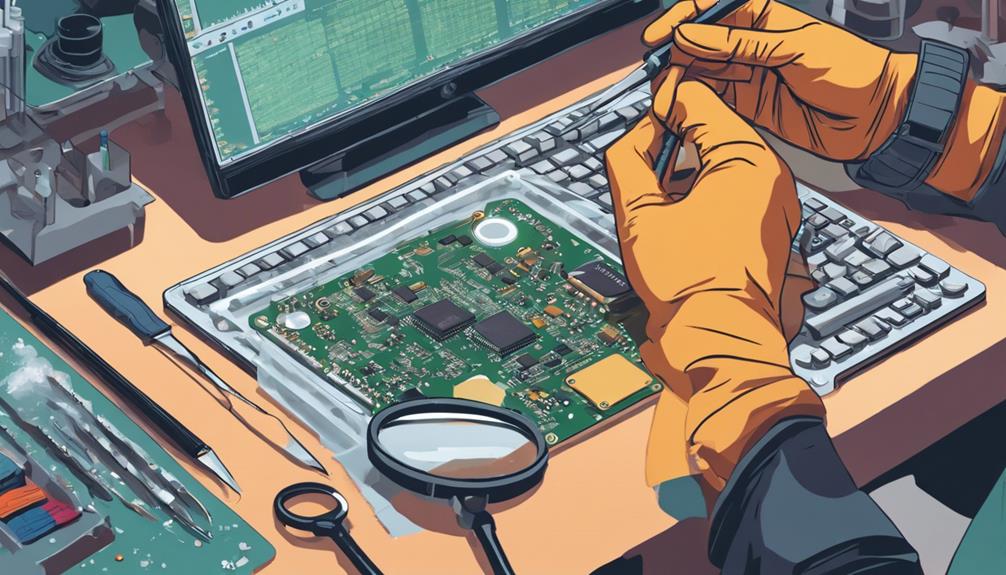
When handling sensitive components, it is vital to exercise extreme care to prevent damage and maintain the integrity of the printed circuit board (PCB).
To achieve this, it is essential to handle components with clean hands, prevent static electricity, and use anti-static materials to minimize the risk of damage.
Handle With Clean Hands
During the fabrication process, it is essential to exercise extreme care when handling sensitive components on a printed circuit board to prevent contamination and damage. Contamination can have a substantial impact on the performance and reliability of the PCB, leading to costly rework or even complete failure.
To prevent contamination and uphold the integrity of the PCB, it is vital to follow proper handling procedures. Here are some essential guidelines to keep in mind:
- Avoid bare-hand contact: Refrain from touching sensitive components on the PCB with bare hands, as oils and sweat can damage the components.
- Use cleanroom practices: Implement cleanroom practices or wear gloves to handle delicate components, preventing contamination and residue buildup.
- Prevent residue buildup: Ensure that handling procedures are designed to prevent residue buildup, which can affect solderability and overall functionality.
- Implement proper handling: Establish and follow proper handling procedures to ensure the longevity and reliability of the printed circuit board.
Prevent Static Electricity
Sensitive components on a printed circuit board are susceptible to damage not only from contamination but also from static electricity, which can be generated by the human body or other sources, making it imperative to handle them with extreme care.
Static electricity can cause electrostatic discharge (ESD), leading to component failure and compromising the reliability of the printed circuit board. To prevent this, it is essential to implement ESD-safe practices when handling sensitive components. This includes using anti-static wrist straps and mats to dissipate static electricity, as well as proper grounding of workstations and tools to prevent static buildup.
By taking these precautions, the risk of ESD-induced component failure can be significantly reduced. Effective handling of sensitive components is vital to ensure the successful fabrication of a printed circuit board.
Use Anti-Static Materials
The careful handling of sensitive components necessitates the use of anti-static materials to prevent electrostatic discharge that can compromise the reliability of the printed circuit board. Electrostatic discharge (ESD) can cause irreversible damage to electronic components, leading to costly rework or replacements.
To prevent ESD damage, it is essential to implement ESD protection measures during PCB fabrication.
Here are some essential tips for using anti-static materials:
- Use ESD-safe workstations and tools to minimize the risk of damaging electronic components.
- Store sensitive components in anti-static bags to prevent ESD damage during storage.
- Use anti-static mats to discharge static electricity from the body before handling sensitive components.
- Implement ESD protection measures throughout the entire PCB fabrication process to guarantee the reliability and performance of the final product.
Drill With Precision and Accuracy

In the pursuit of precision, fabricating a printed circuit board demands a meticulous drilling process that can accurately place holes with exacting dimensions. To achieve drill precision, it is essential to utilize high-quality drill bits with appropriate diameters, ensuring precise hole sizes.
Advanced drilling machines with accurate spindle speeds and feed rates are also critical for consistent results. Proper drill alignment and registration with the PCB are important to avoid errors in hole placement. Additionally, drill depth control mechanisms must be implemented to prevent damage to the underlying layers of the PCB.
Regular drill inspection and maintenance are also necessary to optimize performance and maintain accuracy during the drilling process. By adhering to these guidelines, fabricators can guarantee precise hole placement, minimizing errors and defects in the final product.
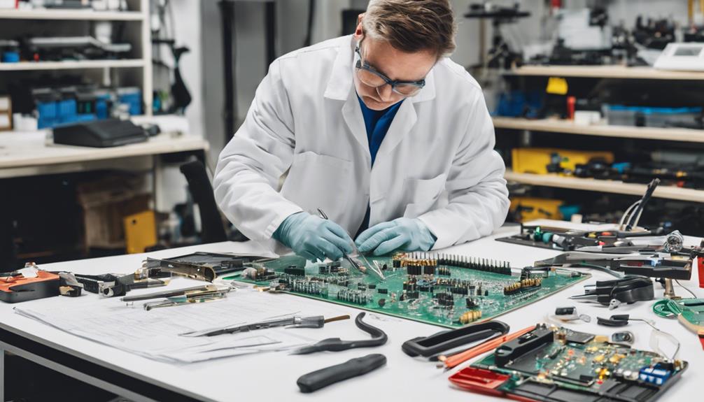
Solder With Skill and Patience

Mastering the art of soldering requires a delicate balance of technique, patience, and attention to detail to guarantee reliable electrical connections and prevent damage to components. In PCB fabrication, soldering is a critical step that demands skill and precision to ensure proper electrical connections.
Patience is key when soldering components onto a PCB to avoid mistakes and ensure a dependable circuit.
To achieve quality soldering, follow these essential guidelines:
- Control the soldering temperature: Confirm the temperature is ideal for the specific solder wire and components to prevent overheating or underheating.
- Select the right soldering tools: Choose a soldering iron with the appropriate wattage and a quality solder wire to achieve clean and strong connections.
- Develop a precise soldering technique: Master a consistent soldering technique to guarantee consistent and reliable solder joints.
- Use the correct soldering materials: Select solder wire and flux that suit the specific components and PCB requirements.
Conduct Regular Quality Control

Regular quality control measures become paramount after the soldering process to guarantee that the PCB meets design specifications and adheres to industry standards.
During the PCB fabrication process, quality control involves a combination of visual inspections, automated optical inspection (AOI), and electrical testing. These measures ensure the PCB meets design specifications, has proper soldering connections, and adheres to industry standards.
By implementing quality control at key stages, such as after solder mask application and before final assembly, the likelihood of defects and costly rework is greatly reduced. Early detection of defects enables prompt correction, ensuring the PCB's reliability and performance.
Consistent quality control practices are essential for producing high-quality PCBs that meet industry standards. By integrating quality control into the fabrication process, manufacturers can guarantee the final product meets the required standards, ensuring excellent performance, functionality, and durability.
Are the Essential Tips for Fabricating a Printed Circuit Board Suitable for Beginners to Master?
When it comes to mastering the fabrication techniques for beginners, it’s important to start with the basics. Understanding the fundamentals of printed circuit board fabrication is crucial for beginners. Learning how to properly handle materials, utilize tools, and follow safety guidelines are essential tips for beginners to master the process.
Adhere to Industry Standards Always
Compliance with industry standards is crucial in guaranteeing the fabrication of high-quality printed circuit boards that meet customer requirements and regulatory expectations. By adhering to industry standards, manufacturers can secure uniformity in fabrication processes and materials used, facilitating interoperability and compatibility with other electronic components.
Here are four key reasons to adhere to industry standards:
- Secures quality and reliability: Following industry standards like IPC-A-600 and IPC-6012 secures quality and reliability in PCB fabrication.
- Guarantees uniformity: Compliance with standards guarantees uniformity in fabrication processes and materials used.
- Facilitates interoperability: Adhering to industry standards facilitates interoperability and compatibility with other electronic components.
- Safeguards against defects: Meeting industry regulations safeguards against defects, errors, and malfunctions in PCB fabrication.
Frequently Asked Questions
What Are the Different Factors to Consider in Designing a Printed Circuit Board?
When designing a printed circuit board, several important factors must be considered. Electrical requirements, signal integrity, and thermal management are essential considerations.
Component placement, routing optimization, and layer stack-up also play a significant role.
Additionally, designers must adhere to design for manufacturability guidelines, incorporate EMI/EMC considerations, and select suitable materials while accounting for environmental factors.
How to Make a Printed Circuit Board Step by Step?
'Getting down to brass tacks,' the step-by-step process of fabricating a printed circuit board involves several important stages.
First, design and layout are finalized, followed by substrate preparation and copper layer deposition.
Next, solder mask application and silkscreen printing occur.
Drilling, plating, and etching ensue, culminating in lamination and quality control measures.
Each step demands precision to guarantee a functional and reliable PCB.
What Are the Basics of Printed Circuit Board?
The basics of a printed circuit board (PCB) involve a substrate material, typically FR4, with copper traces that form the circuit. Insulating layers separate the conductive paths, ensuring electrical isolation.
A solder mask and silkscreen layer facilitate component attachment and labeling. The board's layout and design dictate its functionality, making precise fabrication and quality control essential for reliable performance.
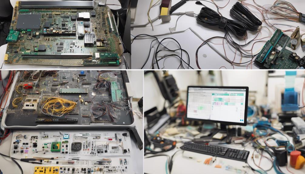
What Are the Steps Involved in PCB Fabrication?
In PCB fabrication, multiple stages are involved to produce a functional board. The process initiates with substrate preparation, followed by copper layer deposition, solder mask application, and silkscreen printing.
Drilling, plating, and etching are subsequent critical steps. Final inspection and quality control measures, including electrical testing and visual inspection, guarantee the board meets design specifications and performs at its best.