
Design for testability is an essential aspect of printed circuit board (PCB) design, ensuring efficient testing, early fault detection, and reduced time and resources for error identification. Effective design for testability involves implementing test points strategically, maintaining clearance and accessibility, and optimizing signal routing. It also includes using test vectors efficiently, designing for manufacturability, and enhancing test coverage and quality. By following essential best practices, designers can guarantee thorough test coverage, reduce testing complexities, and streamline production. As the importance of testability continues to grow, understanding these principles becomes increasingly important for successful PCB design and manufacturing.
Key Takeaways
- Ensure thorough test coverage by incorporating ICT points on every design net and strategically placing test points for accessibility.
- Implement PCB layout strategies that maintain clearance from components, edge clearance, and strategic probe point placement to reduce testing complexity.
- Design for manufacturability by placing ICT points on every design net, ensuring accessible test points with easy clearance, and following DFT guidelines.
- Use efficient test vectors generated through methods like pseudo-random, exhaustive, intelligent, and constraint-based approaches to maximize fault coverage.
- Enhance test coverage and quality by incorporating ICT points, conducting extensive testing, and implementing unit testing to identify manufacturing errors and component failures promptly.
Design for Testability Fundamentals
Design for Testability (DFT) is an essential concept in software and hardware development that emphasizes the creation of components that promote easy testing, thereby guaranteeing better quality and reliability of the final product.
By incorporating DFT principles, developers can create software components that are conducive to various testing types, including unit, integration, functional, load, and performance testing. This holistic approach to testing enables the detection of faults and errors early in the development cycle, reducing the likelihood of downstream problems.
Effective DFT considers the entire testing spectrum, ensuring that components are designed with testability in mind. This approach facilitates quick fault isolation, reducing the time and resources required to identify and rectify manufacturing errors and component failures.
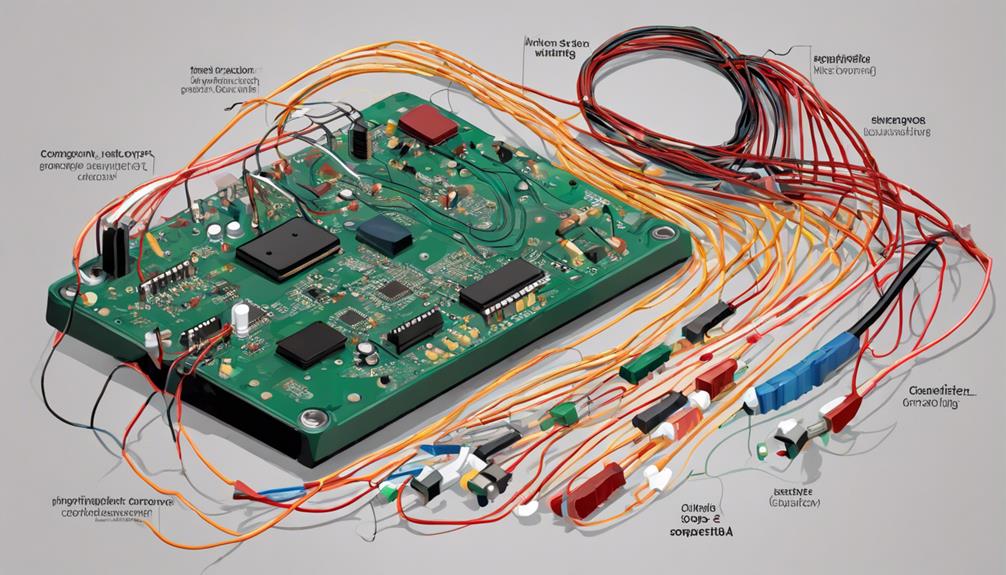
PCB Layout for Maximum Testability
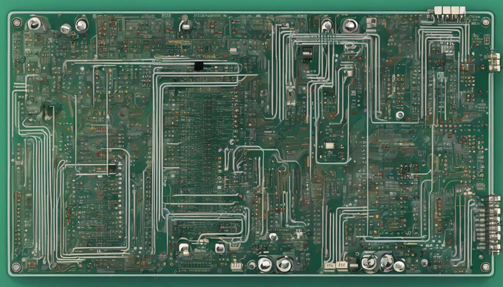
For thorough testability, printed circuit board (PCB) layouts should be designed with intentional test points and accessibility features that facilitate efficient testing and fault diagnosis. A well-designed PCB layout can greatly reduce the complexity and cost of testing.
To achieve maximum testability, the following guidelines should be followed:
- Thorough test coverage: Design PCB layouts with ICT points on each net to guarantee thorough test coverage.
- Clearance from components: Maintain a minimum clearance of 50 mil between test points and components and pads.
- Edge clearance: Maintain a clearance of 100 mil between test points and the board's edge for accessibility.
- Probe point placement: Strategically place probe points for manual testing to facilitate easy access by technicians.
Implementing Test Points Strategically

Strategically positioned test points are essential to guarantee thorough coverage of critical connections on the PCB, facilitating efficient testing and fault diagnosis.
By incorporating test points into the PCB design, engineers can make sure that unit tests are detailed, and faults can be quickly identified and isolated.
To achieve ideal testability, test points should be strategically placed with consideration for accessibility, clearance, and signal integrity requirements. Proper spacing between test points is also critical to prevent short circuits and ensure reliable testing procedures.
Moreover, test points positioned near key components enable efficient fault isolation and troubleshooting during testing.
Effective placement of test points not only simplifies the testing process but also minimizes the complexity of test fixtures, reducing testing costs and time.
Testable Design for Manufacturability

Optimizing PCB layouts for manufacturability necessitates a testable design that integrates ICT points on every design net to guarantee thorough test coverage and facilitate efficient production workflows. This approach enables contract manufacturers (CMs) to conduct ICT testing, ensuring that both sides of the PCB are tested simultaneously.
To guarantee effective testability, the following guidelines should be followed:
- Accessible test points: Guarantee a 50 mil clearance to components and pads for easy accessibility.
- Strategic placement: Position test points based on DFT guidelines to reduce fixture complexity and potential additional costs.
- Easy manual testing: Place probe points for easy accessibility by technicians.
- Coordinated testing: Collaborate with the CM to coordinate ICT testing for efficient production workflows.
Efficient Use of Test Vectors

In the domain of design for testability, efficient use of test vectors is vital for guaranteeing thorough testing of a circuit's functionality.
To achieve this, it is essential to employ effective vector generation methods that can produce a diverse set of test vectors, thereby optimizing test coverage.
Vector Generation Methods
Often, the efficiency of design for testability relies heavily on the effective generation of test vectors, which are essential for verifying the behavior of a design under test (DUT).
In unit testing, test vectors are input patterns used to verify the behavior of a DUT, and their efficient generation is critical for thorough coverage of DUT functionality.
To guarantee efficient testing, various algorithms can be employed for test vector generation. These include:
- Pseudo-random test vector generation, which balances randomness and repeatability for effective testing.
- Exhaustive test vector generation, which involves generating all possible input patterns.
- Intelligent vector generation, which optimizes test coverage while minimizing test time and resources.
- Constraint-based test vector generation, which generates test vectors based on specific constraints and testability guidelines.
Optimizing Test Coverage
Optimizing Test Coverage
Strategic selection of test points is essential for maximizing fault coverage in PCB testing, as it enables the efficient use of test vectors to target specific areas of the design under test. This approach guarantees that potential defects are identified and addressed, reducing the risk of faulty PCBs. Proper allocation of test vectors can greatly reduce testing time while ensuring thorough coverage.
| Optimization Techniques | Benefits |
|---|---|
| Boundary Scan Testing | Enhanced test vector efficiency by accessing internal nodes |
| Test Vector Reuse | Reduced testing time and improved resource allocation |
| Defect-Oriented Testing | Targeted testing of high-fault-probability areas |
| ATPG-based Testing | Efficient fault coverage with automated test pattern generation |
| Hybrid Testing | Combining different techniques for comprehensive coverage |
Simplifying Complex Circuitry Design
Breaking down intricate circuits into smaller, more manageable components is an essential step in simplifying complex circuitry design. This allows designers to tackle each module individually, enhancing overall testability. This approach enables designers to focus on specific modules, reducing the complexity of the overall design.
To achieve this, designers can employ several strategies:
- Modular design: Breaking down complex circuits into reusable modules promotes easier testing and maintenance.
- Reduce dependencies: Minimizing dependencies between components simplifies the design and improves fault isolation.
- Clear documentation: Providing concise and clear documentation of complex circuitry designs facilitates understanding and testing of the design's functionality.
- Design patterns: Implementing design patterns, such as the Observer pattern, can simplify complex circuitry interactions and improve testability.
Effective Signal Routing for Test

When designing for testability, effective signal routing is essential to guarantee accurate measurements, and a well-planned signal routing strategy can greatly reduce errors and enhance testing efficiency.
To achieve this, it is important to minimize signal length to ensure accurate measurements. Moreover, differential signal pairs should be routed together to maintain signal integrity during testing. This prevents signal degradation and ensures reliable test results.
In addition, it is vital to avoid routing signals near noisy components to prevent interference during testing. Controlled impedance traces should be used to maintain signal integrity and accuracy during testing. This ensures that the test signals are not distorted, providing reliable test results.
Implementing test points at strategic locations is also critical for easy access and efficient testing processes. By incorporating these design considerations, designers can make sure that their signal routing strategy is optimized for testability, resulting in efficient and accurate testing.
Effective signal routing is a critical aspect of design for testability, and by following these best practices, designers can ensure reliable and efficient testing.
Designing for In-Circuit Testing

When designing printed circuit boards (PCBs) for in-circuit testing (ICT), careful consideration must be given to the placement of components, identification of test points, and signal routing to guarantee efficient and effective testing. By optimizing these factors, designers can facilitate ICT coverage and rapid fault isolation, ultimately reducing production costs and improving product quality.
In the following sections, we will examine the key points of accessible component placement, test point identification, and signal routing considerations that enable successful ICT.
Accessible Component Placement
Proper accessible component placement is essential in designing for in-circuit testing, as it enables efficient test point placement and guarantees thorough test coverage. This is critical for unit testing, as it ensures that the design code can be tested comprehensively.
In ICT testing, test points are strategically placed to facilitate easy access for testing equipment and technicians, reducing testing complexities.
To achieve ideal component placement, designers should consider the following guidelines:
- Clearance requirements: Ensure 50 mil clearance to components and 100 mil clearance to the edge of the board.
- Test point placement: Strategically locate test points on the PCB layout, considering clearance requirements for efficient testing.
- Component accessibility: Ensure components are accessible for testing purposes, reducing testing complexities.
- Efficient test coverage: Guarantee thorough test coverage by placing test points in a way that enables comprehensive testing.
Test Point Identification
In the pursuit of efficient in-circuit testing, test point identification plays a pivotal role in PCB design, as it enables the strategic placement of dedicated points on the board for ICT. This deliberate placement of ICT test points ensures that they are easily accessible, with sufficient clearance from components and board edges, allowing for efficient testing during production.
Proper spacing between test points is also essential, as it ensures accurate and efficient testing. These test points facilitate the connection of ICT fixtures, enabling automated testing processes.
Additionally, well-placed and labeled test points enable quick fault isolation and debugging during ICT, facilitating the identification and rectification of issues. Effective test point identification in PCB design is crucial for efficient in-circuit testing, streamlining the testing process, and reducing production time.
Signal Routing Considerations
Signal routing considerations play a critical role in designing for in-circuit testing, as they directly impact the accuracy and reliability of test results. Proper signal routing is essential for ensuring efficient testing of PCBs. In ICT, signal path lengths should be minimized, and controlled impedance routing should be utilized to prevent signal degradation.
To achieve reliable testing, the following signal routing considerations should be taken into account:
- Minimize crossovers: Avoid crossing signals over each other to prevent electromagnetic interference and signal degradation.
- Avoid sharp bends: Use smooth, curved routes to prevent signal reflections and radiation.
- Limit vias: Minimize the use of vias to prevent signal loss and degradation.
- Strategic test point placement: Place test points strategically to facilitate easy access for testing probes, ensuring efficient and reliable testing.
Enhancing Test Coverage and Quality

Effective test strategies, such as incorporating ICT points on each design net, are vital for guaranteeing thorough test coverage and quality in PCB manufacturing. This approach enables extensive testing, reducing the likelihood of manufacturing errors and component failures going undetected.
By including test points with adequate clearance from components and the board's edge, technicians can efficiently conduct unit testing and identify issues promptly. Additionally, ICT can be conducted simultaneously on both sides of the board with coordination from the contract manufacturer, streamlining the testing process.
Moreover, having easily accessible probe points for manual testing simplifies testing procedures, reducing the risk of human error. Critical test coverage and quality assurance are essential in identifying manufacturing errors and component failures promptly, ensuring that only high-quality PCBs are released to the market.
Optimizing PCB Design for Test

When optimizing PCB design for test, it is vital to take into account the placement of test points, ensuring that they are easily accessible for efficient testing.
Proper test point placement facilitates thorough test coverage, reduces testing time, and increases test quality.
Design for Accessibility
A well-designed PCB layout that incorporates accessible test points enables efficient testing processes, reducing the time and cost associated with identifying and rectifying defects. Design for accessibility is a critical aspect of optimizing PCB design for test, as it facilitates the testing process and ensures thorough fault coverage.
To achieve ideal accessibility, designers should consider the following key factors:
- Clearance from components and board edges: Ensure test points have sufficient clearance to allow easy access for testing probes.
- ICT points on each design net: Incorporate ICT points on each design net to enable thorough test coverage during manufacturing.
- Collaboration with contract manufacturers: Work with contract manufacturers to determine the most effective test methodologies and fixture modifications for enhanced fault coverage.
- ICT testing for immediate feedback: Utilize ICT testing to receive immediate feedback on manufacturing errors, component failures, and overall PCB functionality, enabling quick adjustments.
Test Point Placement
Strategically placing test points on a PCB is essential for maximum coverage during ICT testing, as it enables efficient fault detection and isolation during manufacturing. Effective test point placement is critical for optimizing PCB design for testability. By following DFM guidelines, designers can determine the ideal locations for test points on the PCB, ensuring ideal coverage and facilitating fault detection.
Proper clearance from components and board edges is also vital to facilitate testing processes. Well-placed test points enable quick and accurate testing, leading to improved overall product quality. ICT testing requirements should be considered during the design phase to ensure test points are strategically placed for maximum coverage.
Frequently Asked Questions
What Are the Principles of Design for Testability?
The principles of design for testability revolve around crafting code that is modular, loosely coupled, and easy to test. This is achieved by adhering to principles such as Single Responsibility, Open/Closed, Liskov Substitution, Interface Segregation, and Dependency Inversion.
Additionally, test-driven development, refactoring, and minimizing dependencies are essential for creating testable code. By following these principles, developers can write code that is maintainable, scalable, and easy to test, resulting in improved code quality and reduced technical debt.
What Are DFT Techniques?
While traditional PCB design focuses on aesthetics and functionality, a paradigm shift is necessary to prioritize testability.
DFT techniques are a deliberate design approach that integrates testing considerations into the PCB layout. These techniques include strategically placing test points, using boundary scan techniques, and implementing built-in self-test (BIST) capabilities.
What Are PCB Guidelines in Testing?
PCB guidelines in testing outline specific requirements for test point placement and clearance on printed circuit board layouts. These guidelines guarantee efficient fault isolation and testing during PCB manufacturing, streamlining the testing process and improving fault detection.
Why Is DFT Required?
Design for Testability (DFT) is an essential aspect of PCB design. It enables efficient fault detection and isolation during manufacturing, reducing production costs and time-to-market. By incorporating DFT principles, manufacturers can guarantee high-quality products, minimize defects, and streamline testing processes.
Effective DFT implementation facilitates rapid identification and resolution of faults. This ultimately leads to improved product reliability and customer satisfaction.

