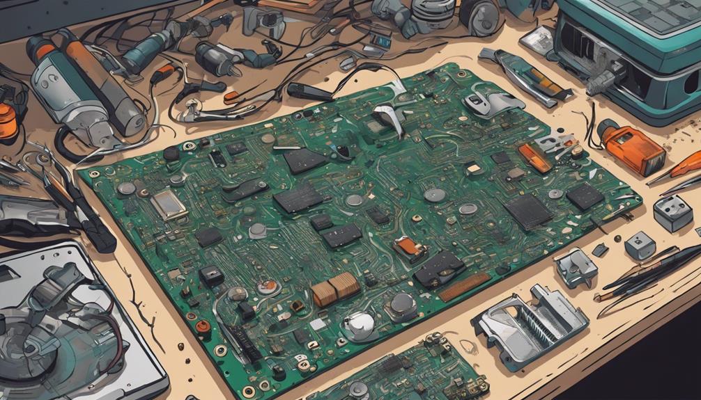
Printed circuit board (PCB) failures can be attributed to a multitude of factors, including plating voids, inadequate copper clearance, slivers, and solder mask issues. Poor manufacturing processes, design flaws, and environmental factors such as heat, dust, and moisture can also contribute to PCB failure. Additionally, acid traps, soldering problems, and manufacturing defects can compromise PCB reliability. Understanding the root causes of PCB failure is vital for designing and manufacturing reliable electronic systems. By examining these factors, it becomes evident that a thorough approach to PCB design and manufacturing is essential for preventing failures and ensuring top-notch performance.
Key Takeaways
- Plating voids, poor plating processes, and contamination can lead to unreliable connections and PCB failure.
- Inadequate copper clearance and design flaws can cause short circuits and unintended current flow.
- Slivers, acid traps, and manufacturing defects can cause short circuits, corrosion, and device failures.
- Soldering problems, such as cold solder joints, and solder mask issues can compromise connections and PCB longevity.
- Environmental factors, including heat, dust, and moisture, can degrade and cause PCB failure over time.
Plating Voids and Unreliable Connections
Plating voids, which manifest as empty spaces in the copper plating on printed circuit boards, are a common culprit behind unreliable electrical connections and subsequent PCB failures. These voids can occur due to poor plating processes, inadequate adhesion, or contamination during manufacturing, leading to compromised copper plating integrity. As a result, electrical connections become unreliable, causing signal loss, intermittent failures, and overall PCB malfunction.
To identify plating voids, diagnostic techniques such as micro-sectioning analysis and X-ray inspection are employed. These methods enable manufacturers to detect and address plating voids, ensuring proper functionality and reliability of printed circuit boards.
In PCB manufacturing, it is important to implement quality control measures to prevent plating voids from occurring in the first place. By doing so, manufacturers can minimize the risk of unreliable connections and signal loss, ultimately preventing PCB failures.
Copper Clearance and Short Circuits
Inadequate copper clearance, a critical design consideration in printed circuit board manufacturing, can have devastating consequences, including short circuits that can render the entire board non-functional. Copper clearance refers to the minimum distance between copper traces or components on a PCB. Insufficient spacing between these elements can lead to short circuits, resulting in unintended current flow and potentially catastrophic failure.
Proper PCB design and layout considerations for copper clearance are essential to prevent short circuits. Implementing design rules for copper clearance can help avoid short circuits and guarantee the reliability of the printed circuit board. Short circuits can damage components, disrupt signal flow, and ultimately render the PCB non-functional.
To mitigate this risk, designers must carefully consider copper clearance in their designs, ensuring adequate spacing between copper traces and components to prevent unintended current flow. By following established design rules and guidelines, PCB designers can minimize the risk of short circuits and secure the reliable operation of their printed circuit boards.
Slivers and Electrical Interference
As printed circuit boards are manufactured, small fragments of conductive material, known as slivers, can be inadvertently left behind, posing a significant threat to the reliability of the PCB. These slivers can cause short circuits and disrupt electrical signals, leading to erratic behavior in electronic devices. The electrical interference generated by slivers can have devastating consequences, including device malfunction and failure.
Slivers are a common byproduct of PCB manufacturing, and their presence can be attributed to inadequate quality control processes. During the manufacturing process, small pieces of conductive material can break off and remain on the board, waiting to cause havoc.
It is essential to implement rigorous inspection and testing procedures to identify and eliminate slivers on PCBs. By doing so, manufacturers can greatly reduce the risk of PCB failure and uphold the reliability of their products. Effective quality control measures can help detect and remove slivers, minimizing the likelihood of electrical interference and short circuits.
Missing Solder Mask and Component Damage

Frequently, the absence of a solder mask can have far-reaching consequences for the reliability and longevity of a printed circuit board, ultimately leading to premature failure. A missing solder mask exposes copper traces to potential short circuits and corrosion, compromising the PCB's electrical conductivity.
Additionally, the lack of a protective layer between components and the environment increases the risk of component damage. This can occur due to exposure to environmental stressors, such as moisture, heat, and contaminants.
The absence of a solder mask can also lead to acid traps, which can cause long-term damage to the PCB. Moreover, the lack of solder mask between pads can result in poor soldering connections, reducing the overall electrical conductivity of the PCB.
Proper application of solder mask is essential for protecting components and ensuring the longevity of the PCB. By neglecting this critical step, manufacturers risk compromising the reliability and performance of their PCBs, ultimately leading to premature failure.
Acid Traps and Corrosion Risks
Beyond the risks associated with missing solder masks, another common cause of printed circuit board failure lies in the formation of acid traps, which can lead to corrosion and compromise the reliability of electronic devices.
Acid traps occur when etchant is unintentionally trapped during the PCB manufacturing process, creating areas where corrosion can occur over time. If left unchecked, these acid traps can lead to short circuits and failures in electronic devices.
The corrosion risks associated with acid traps can compromise the functionality and lifespan of electronic components on the PCB. To safeguard against these risks, proper PCB design and manufacturing processes are essential.
Designers and manufacturers must take steps to prevent acid traps from forming, and regular inspection and maintenance can help identify and address these issues before they result in PCB failure.
Thermal Stress and PCB Malfunctions
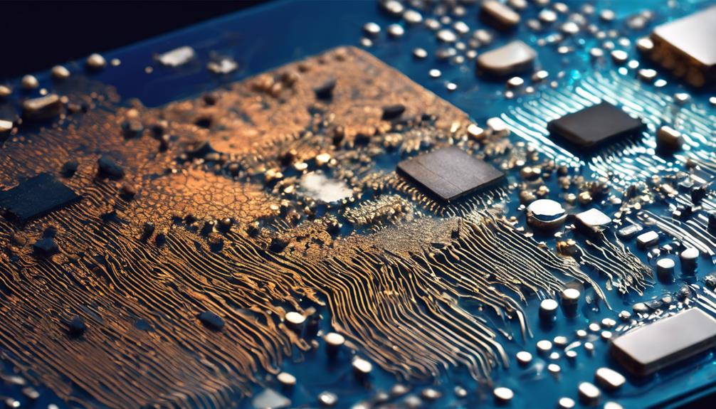
Thermal stress is a pervasive culprit in printed circuit board (PCB) failure. It can be attributed to excessive temperature fluctuations and suboptimal material selection. Temperature extremes, in particular, can wreak havoc on PCBs, causing components to malfunction or fail altogether.
As we explore the nexus of thermal stress and PCB malfunctions, we will examine the critical role of material selection and temperature extremes in mitigating this pervasive issue.
Temperature Extremes Matter
Under conditions of extreme heat or cold, printed circuit boards are susceptible to thermal stress, a primary catalyst for PCB malfunctions and failures.
Temperature extremes can lead to heat stress, causing components to expand and contract at different rates, resulting in weakened solder joints and increased likelihood of failure.
The proper weight of copper and plating plays a vital role in reducing thermal stress on PCB components, ensuring dependable performance.
Burned out components on a PCB are easily identifiable signs of thermal stress-related issues, which can be catastrophic for high-performance applications.
Effective heat dissipation is essential to mitigate thermal stress and prevent failures.
By understanding the impact of temperature extremes on PCBs, designers and manufacturers can take proactive measures to secure the reliability and longevity of their products.
Material Selection Errors
Inadequate consideration of material properties during the design phase can lead to mismatches in thermal expansion rates, exacerbating thermal stress and increasing the likelihood of PCB malfunctions. Material selection errors can result in thermal stress, leading to malfunctions and failures in printed circuit boards. This stress can weaken solder joints, causing them to fail prematurely.
| Material Property | Thermal Expansion Rate | Consequence of Mismatch |
|---|---|---|
| Copper | 16.5 ppm/K | Weakened solder joints |
| FR4 | 12-14 ppm/K | Thermal stress and PCB malfunction |
| Solder | 21-25 ppm/K | Cracked or broken joints |
| Plating | 10-15 ppm/K | Reduced lifespan and reliability |
High-performance PCBs require effective heat dissipation to reduce the impact of thermal stress. Incorrect weight of copper and plating issues can exacerbate thermal stress, leading to burned out components and PCB malfunctions. By understanding the material expansion rates and their consequences, designers can make informed decisions to minimize thermal stress and guarantee reliable PCB performance.
Poor Soldering and Joint Failures

Poor soldering and joint failures can lead to Printed Circuit Board (PCB) malfunctions and failures.
Cold solder joints, formed due to inadequate solder flow, are a common issue that can compromise the integrity of the connections on the PCB.
Inadequate solder flow can result in weak joints, increasing the likelihood of PCB failure.
Cold Solder Joints Form
Insufficient heat or improper soldering techniques can cause solder to form a weak bond with components, resulting in cold solder joints that compromise the reliability of printed circuit boards.
Cold solder joints are a common issue in PCB manufacturing, leading to intermittent electrical connections, circuit failures, and overall malfunction. The primary causes of cold solder joints are insufficient heat during soldering and improper technique, resulting in weak joints.
| Causes | Effects |
|---|---|
| Insufficient heat | Weak joints, intermittent connections |
| Improper technique | Cold solder joints, circuit failures |
| Inadequate training | PCB malfunction, reliability issues |
To identify cold solder joints, visual inspection and testing with a multimeter can help detect the issue for repair. It is essential to employ proper soldering techniques, equipment, and training to prevent cold solder joints and ensure reliable PCB performance. By understanding the causes and effects of cold solder joints, manufacturers can take proactive measures to prevent these defects and uphold the quality of their printed circuit boards.
Inadequate Solder Flow
During the soldering process, the flow of solder can be compromised, leading to weak joints and potential circuit board failure, further underscoring the importance of proper soldering techniques.
Inadequate solder flow can result in weak joints, prone to cracking and breaking under stress, causing intermittent electrical connections and system malfunctions. Insufficient solder flow can also lead to cold solder joints, which are notoriously unreliable and prone to failure.
To mitigate these risks, it is essential to employ proper soldering techniques, ensuring sufficient solder flow and strong, reliable connections on the printed circuit board (PCB).
Quality control measures during soldering processes are vital to prevent inadequate solder flow and potential board failures. By implementing rigorous quality control measures, manufacturers can minimize the risk of inadequate solder flow and ensure the production of high-quality, reliable PCBs.
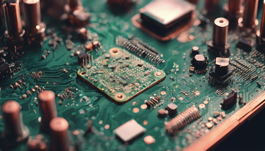
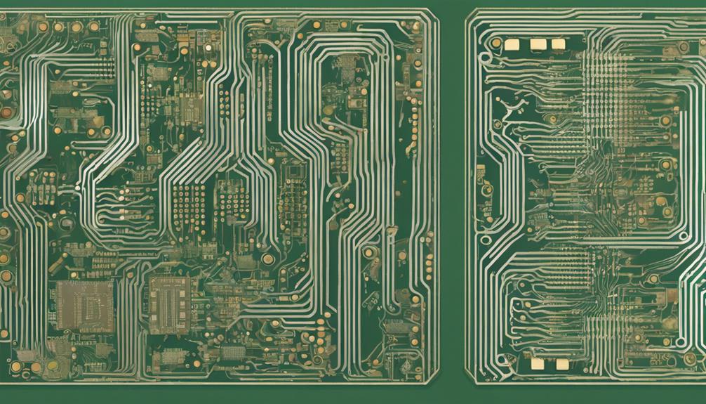
Manufacturing Defects and PCB Failure
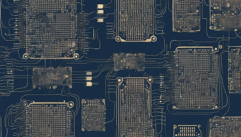
Manufacturing defects, responsible for the majority of printed circuit board failures during the assembly process, can manifest in various forms, including misaligned layers, short circuits, and crossed signals. These defects can lead to catastrophic failures, rendering the PCB unusable. To mitigate these issues, it is essential to implement robust quality control measures during the fabrication and manufacturing process.
| Manufacturing Issue | Description | Impact on PCB |
|---|---|---|
| Misaligned layers | Layers of the PCB not properly aligned, leading to short circuits | PCB failure, reduced performance |
| Short circuits | Unintended connections between PCB components | PCB failure, reduced performance |
| Crossed signals | Signals transmitted between incorrect components | PCB failure, reduced performance |
| Contaminated solder | Impurities in the solder, affecting joint quality | PCB failure, reduced reliability |
| Improper soldering techniques | Incorrect soldering methods, leading to weak joints | PCB failure, reduced reliability |
Proper PCB testing and inspection during the assembly process can help identify and rectify these manufacturing issues, ensuring the production of high-quality PCBs. By addressing these defects, manufacturers can minimize PCB failures and guarantee reliable performance.
Environmental Factors and PCB Degradation
As printed circuit boards are inherently susceptible to environmental stresses, exposure to heat, dust, and moisture can lead to degradation and potential failure.
Environmental factors, such as extreme temperatures, can accelerate PCB degradation, causing thermal stress and potential component failure.
Foreign debris like dust, hair, liquid, and fibers can cause overheating and degrade PCB performance over time.
To mitigate these risks, climate-controlled manufacturing environments are recommended to maintain safe humidity levels and prevent environmental factors from affecting PCBs.
Accidental impacts, power overloads, surges, and electrostatic discharge (ESD) can contribute to PCB failures.
The accumulation of these environmental factors can lead to PCB degradation, ultimately resulting in failure.
It is essential to take into account these environmental factors during the design and manufacturing process to ensure the reliability and longevity of printed circuit boards.
Design Flaws and PCB Inefficiencies
Inherent design flaws and inefficiencies can greatly compromise the reliability and performance of printed circuit boards, leading to premature failure or malfunction.
PCB design flaws, such as plating voids and insufficient copper-to-edge clearance, can lead to circuit board failures. Additionally, missing solder mask between pads and acid traps are common design inefficiencies that can impact PCB performance.
Inadequate shielding from electromagnetic interference due to design oversights can cause PCB malfunctions. Improper layout planning and soldering errors resulting from design flaws can also contribute to PCB failure.
To mitigate these issues, it is essential to utilize Design-For-Manufacturing (DFM) software and prototype testing to identify and rectify design flaws in PCBs. By doing so, manufacturers can make sure that their PCBs meet the required standards, minimizing the risk of failure and ensuring efficient performance.
Frequently Asked Questions
What Is the Main Cause of PCB Failure?
The primary culprit behind printed circuit board (PCB) failure is defects introduced during the assembly process.
These defects can manifest in various forms, including misaligned layers, short circuits, and crossed signals.
Such flaws can lead to catastrophic failures, underscoring the significance of quality control measures during PCB assembly to guarantee reliable performance and minimize the risk of malfunction.
What Are the Failure Modes of Printed Circuit Boards?
What lies at the heart of printed circuit board unreliability?
The failure modes of printed circuit boards encompass a broad spectrum of defects and malfunctions. These include defects introduced during assembly, burnt components, environmental factors such as heat and humidity, soldering issues, and human errors.
Each of these failure modes can have devastating consequences, including component malfunction, data loss, and system crashes.
Understanding these failure modes is vital to designing and manufacturing reliable printed circuit boards.
What Are the Common Defects in Pcb?
In the domain of printed circuit board (PCB) manufacturing, common defects can greatly impact product reliability. Misaligned layers, short circuits, and crossed signals are prevalent defects that can lead to PCB failure. These defects are often sensitive to electrostatic discharge (ESD), which can exacerbate the issue.
Ensuring proper precautions, such as ESD-safe materials and trained personnel, can mitigate these defects, resulting in higher-quality PCBs.
What Are Two Common Problems When Troubleshooting a Circuit Board?
When troubleshooting a circuit board, two pervasive problems often emerge: burnt components and soldering issues. These issues can be attributed to various factors, including excessive heat, improper spacing, and component failure. Contaminated solder and faulty connections further exacerbate these problems.
Identifying and addressing these issues is essential to resolving circuit board failures. By understanding the root causes of these problems, effective troubleshooting and resolution can be achieved, ensuring the reliability and performance of the circuit board.