Accurate RF circuit performance is maintained by adhering to a set of rigorous design rules. These include PCB design rule checks, material selection guidelines that consider dielectric loss and thermal properties, and strategic component placement to minimize signal degradation. Impedance matching techniques, such as transmission line transformers and stub matching, are also essential. Moreover, transmission line design rules, including controlled impedance and proper termination, are crucial. Finally, grounding and shielding strategies, such as star grounding and Faraday cages, are important. By following these guidelines, designers can optimize their RF circuit designs for peak performance, and uncovering the intricacies of each rule will reveal even more opportunities for improvement.
Key Takeaways
- Ensure adherence to signal integrity guidelines and verify impedance matching requirements to prevent signal distortions and reflections.
- Select materials with low dielectric loss, such as Rogers or Taconic, to maintain consistent impedance and minimize signal degradation.
- Implement transmission line design rules, including controlled impedance and proper termination, to maintain signal integrity and minimize reflections.
- Employ grounding and shielding strategies, including star grounding, solid ground planes, and shielding methods, to reduce interference and electromagnetic interference.
- Verify component placement strategies, such as separating RF components from digital circuits, to minimize crosstalk and optimize RF circuit performance.
PCB Design Rule Checks
Rigorously implementing PCB design rule checks is essential to guarantee adherence to signal integrity guidelines, impedance matching requirements, and manufacturing constraints, thereby securing accurate RF circuit performance. These checks verify that the design meets the necessary standards, ensuring that the RF circuit operates as intended.
By identifying issues such as trace width violations, clearance violations, and inadequate ground connections, design rule checks prevent signal distortions, reflections, crosstalk, and EMI in RF circuits. Additionally, checking for correct via placement, controlled impedance paths, and proper layer stack-up is critical for efficient RF circuit functionality.
Implementing design rule checks early in the design process aids in detecting and correcting potential RF circuit performance issues before fabrication. This proactive approach enables designers to create reliable, high-performance RF circuits that meet the required signal integrity guidelines, impedance matching requirements, and manufacturing constraints.
Material Selection Guidelines
Just as PCB design rule checks guarantee the integrity of the circuit's physical structure, the selection of suitable materials for the RF PCB is equally important, as it directly impacts the circuit's electrical performance. RF material selection is critical for achieving peak RF circuit performance. The choice of material affects dielectric loss, impedance matching, and signal distortion, ultimately influencing signal integrity.
| Material Property | Impact on RF Performance |
|---|---|
| Dielectric Loss | Signal Attenuation, Distortion |
| Substrate Dielectric Constant | Impedance Matching, Signal Velocity |
| Thermal Properties | Operating Temperature, Reliability |
To ensure accurate RF circuit performance, engineers should select high-frequency laminates like Rogers or Taconic materials for RF PCB designs. These materials exhibit low dielectric loss and consistent impedance characteristics, which are essential for minimizing signal loss and ensuring dependable RF circuit operation. By considering substrate dielectric constant, loss tangent, and thermal properties, engineers can make informed material selection decisions that guarantee peak RF circuit performance.
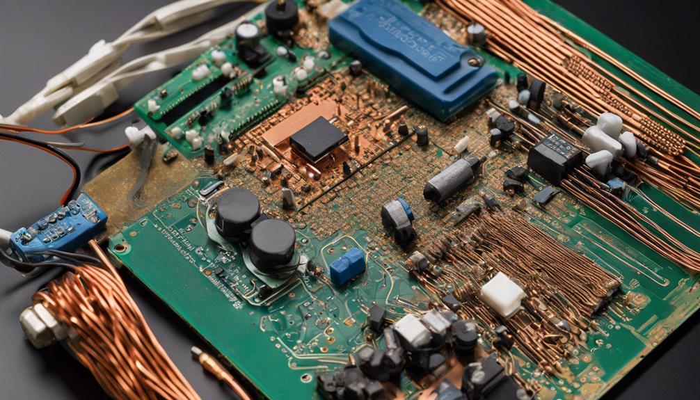
Component Placement Strategies
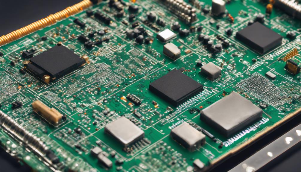
When implementing Component Placement Strategies, careful consideration must be given to the orientation of components to minimize signal degradation and maximize performance.
Additionally, signal path minimization techniques can be employed to reduce parasitic effects and optimize signal integrity.
Optimal Component Orientation
By strategically orienting components, RF circuit designers can greatly minimize parasitic effects, electromagnetic interference, and transmission line losses, ultimately optimizing overall circuit performance. This is achieved by carefully considering the placement of each component to reduce signal interference and enhance RF circuit performance.
To achieve ideal component orientation, designers should:
- Separate sensitive RF components from noisy digital circuits to minimize parasitic effects and electromagnetic interference (EMI).
- Keep analog and digital sections separate to reduce crosstalk and EMI.
- Place RF components closer to the antenna and use shorter traces to minimize transmission line losses.
- Consider thermal management during component placement to efficiently dissipate heat and maintain ideal performance.
Signal Path Minimization
Key signal path minimization, an important aspect of RF circuit design, involves strategically placing components to reduce transmission line losses and signal degradation, thereby guaranteeing accurate RF circuit performance and signal integrity.
By minimizing signal path length, designers can greatly decrease transmission line losses and signal degradation, resulting in improved RF circuit performance. Strategic component placement near the antenna minimizes interference and enhances signal quality, while shorter trace lengths decrease parasitic effects and boost RF circuit performance.
In addition, placing RF components closer together optimizes signal flow and reduces crosstalk, ensuring precise signal transmission. Efficient component placement strategies guarantee accurate RF circuit performance and signal integrity by reducing transmission line losses, minimizing interference, and enhancing signal quality.
Decoupling Capacitor Placement
In high-frequency RF circuits, strategically placing decoupling capacitors in close proximity to the power pins of active components is essential for minimizing noise and voltage fluctuations that can compromise signal integrity. This intentional placement is vital for ensuring peak RF circuit performance.
Here are key considerations for effective decoupling capacitor placement:
- Minimize distance to power pins: Place decoupling capacitors as close as possible to the power pins of active RF components to reduce noise and voltage fluctuations.
- Optimize power distribution: Strategically place decoupling capacitors near high-power RF components to improve power distribution and reduce signal distortion.
- Act as energy reservoirs: Decoupling capacitors absorb and supply instantaneous current demands, maintaining stable RF circuit operation.
- Enhance signal integrity: Effective decoupling capacitor placement minimizes voltage fluctuations and reduces electromagnetic interference, ensuring consistent RF circuit performance.
Impedance Matching Techniques

Optimizing the transfer of RF signals between components requires the strategic application of impedance matching techniques to guarantee maximum power transfer and minimal signal loss. This is important in RF circuit design, as impedance mismatching can lead to significant signal reflections, loss, and distortion.
To mitigate these issues, designers employ impedance matching techniques, such as transmission line transformers and lumped element matching networks. These methods ensure proper impedance matching, minimizing signal reflections and maximizing power transfer efficiency.
Additionally, stub matching techniques can be utilized to achieve impedance matching and suppress harmonics in RF circuits. Accurate impedance matching is vital for minimizing signal distortion and maximizing RF circuit performance.
Transmission Line Design Rules
What sets transmission line design apart from other RF circuit components is the critical need to maintain controlled impedance for signal integrity, as even slight deviations can lead to signal reflections and distortion.
Transmission line design rules are vital to ensuring accurate RF circuit performance, and neglecting these rules can result in signal loss and degradation.
To achieve efficient transmission, the following transmission line design rules must be adhered to:
- Maintain controlled impedance: Make sure that the transmission line's impedance is consistent throughout the circuit to prevent signal reflections and distortion.
- Proper termination: Terminate transmission lines correctly to minimize reflections and signal loss.
- Optimize transmission line length: Length should be optimized to reduce signal distortion and ensure efficient transmission.
- Implement impedance matching techniques: Techniques like stub matching should be employed to guarantee impedance matching and accurate RF circuit performance.
Grounding and Shielding Methods

While transmission line design rules are essential for maintaining signal integrity, proper grounding and shielding methods are equally vital for preventing electromagnetic interference and guaranteeing accurate RF circuit performance. Grounding techniques, such as star grounding and solid ground planes, help minimize interference by reducing ground loops and impedance. These techniques create a continuous ground plane, guaranteeing that RF circuits operate accurately in high-frequency applications.
Shielding methods, including Faraday cages and metal shielding enclosures, block external electromagnetic interference, preventing signal degradation and ensuring accurate RF circuit operation. Additionally, grounding vias and stitching help create a continuous ground plane, while shielding techniques like RF gaskets and shielded cables contain RF signals and prevent electromagnetic interference in sensitive circuitry.
Frequently Asked Questions
How to Design an RF Circuit?
To design an RF circuit, start by developing a high-level specification outlining performance requirements, such as frequency range, power levels, and noise tolerance.
Next, create a device-level circuit description, selecting suitable components and materials. Utilize simulation tools to verify the design, followed by physical layout implementation and testing to validate performance.
Throughout the process, adhere to established design rules and guidelines to guarantee accurate RF circuit performance.
What Are Basic Checks for RF Design?
Did you know that 75% of RF circuit failures can be attributed to poor design and inadequate testing?
When it comes to basic checks for RF design, there are several key considerations. Foremost, impedance matching is vital to guarantee proper signal transmission and reception.
Additionally, proper grounding and shielding are essential to minimize electromagnetic interference.
What Is RF in Layout Design?
RF in layout design refers to the deliberate placement and routing of radio frequency components on a printed circuit board (PCB) to guarantee peak performance.
This involves strategic component placement, precise trace routing, and controlled impedance to minimize signal loss and electromagnetic interference.
What Are the Considerations of RF Pcb?
When designing RF PCBs, several key considerations play a significant role in achieving peak performance. Material selection is essential, as it greatly impacts signal propagation and loss.
Component placement is crucial, as it directly influences signal flow, interference, and overall performance.
Trace design and impedance matching are pivotal for signal integrity, while via size and grounding techniques maximize system efficiency.
Additionally, the loss tangent of materials must be taken into account to minimize signal loss, ensuring accurate RF circuit performance.