
Effective high-frequency circuit design relies on optimizing signal path lengths, strategic component placement, and controlling trace impedance. Minimizing signal path lengths reduces propagation delays and signal degradation. Strategic component placement minimizes interference and guarantees signal integrity, with sensitive components placed away from noise sources. Controlled impedance traces prevent signal reflections and degradation. By mastering these essential layout tips, designers can achieve peak performance in high-frequency circuit design. As the complexity of high-frequency circuits continues to evolve, understanding these fundamental principles is essential for achieving superior circuit performance.
Key Takeaways
- Minimize signal path lengths to reduce propagation delays and ensure signal quality and reliability in high-frequency circuits.
- Strategically place components to minimize signal interference, reduce trace lengths, and optimize signal paths for high-frequency circuits.
- Control trace impedance by calculating trace width based on the dielectric constant to prevent signal reflections and ensure signal integrity.
- Place sensitive components away from noise sources and high-frequency components closer together to reduce interference and optimize signal paths.
- Use proper layout techniques to optimize component placement and routing signals, ensuring signal integrity and reducing delays in high-frequency circuits.
Optimizing Signal Path Lengths
When designing high-frequency circuits, minimizing signal path lengths is essential to prevent signal degradation and maintain signal integrity. In High Frequency PCB Design, optimizing signal path lengths is vital to guarantee efficient signal transmission.
Longer trace lengths can introduce impedance mismatches, leading to signal degradation and interference. To mitigate this, PCB designers should focus on minimizing signal path lengths to reduce signal propagation delays.
This can be achieved through the implementation of proper layout techniques, such as optimizing component placement and routing signals in a way that minimizes trace lengths. By doing so, designers can maintain signal integrity, reduce interference, and ensure reliable signal transmission.
Optimization of signal path lengths is critical for high-frequency circuit performance, as it directly impacts signal quality and reliability. By prioritizing signal path length optimization, designers can create high-performance circuits that meet the demands of modern high-frequency applications.
Strategic Component Placement
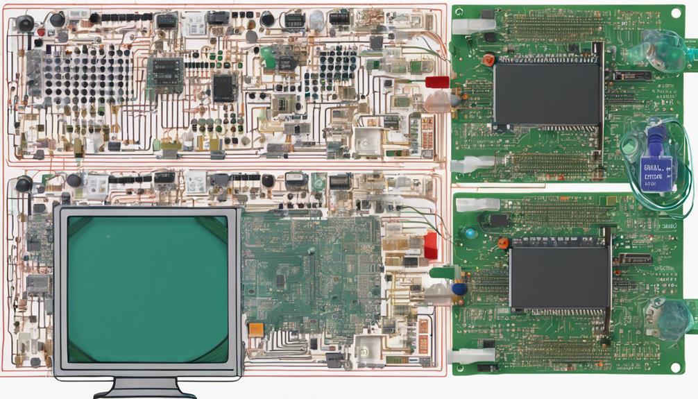
In high-frequency circuit design, strategic component placement is essential, as it enables the minimization of signal interference and guarantees signal integrity by reducing trace lengths and signal delays. By carefully arranging components, designers can optimize signal paths, reducing transmission line lengths and minimizing parasitic capacitance and inductance effects.
| Component | Placement Considerations | Benefits |
|---|---|---|
| High-Frequency Components | Place closer to each other | Reduces signal interference and transmission line lengths |
| Sensitive Components | Place away from noise sources | Minimizes signal interference and improves signal quality |
| Critical Signal Paths | Optimize component placement for shortest paths | Reduces signal delays and improves signal integrity |
Strategic component placement is essential in high-frequency circuit design, as it directly impacts signal quality and integrity. By minimizing signal interference and reducing transmission line lengths, designers can ensure reliable signal transmission and maintain signal integrity. By following these guidelines, designers can create high-frequency circuits that deliver high-quality signals and minimize the risk of crosstalk.
Controlling Trace Impedance
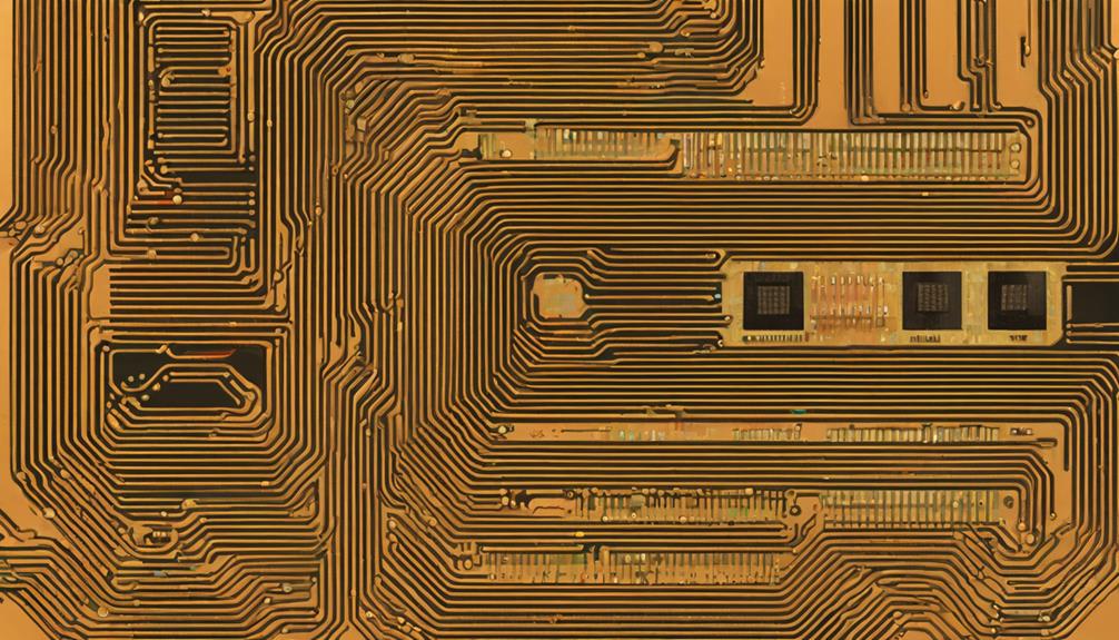
Managing trace impedance is fundamental in high-frequency circuit design, as it directly impacts signal reflection, transmission, and overall circuit performance. In high-frequency PCB design, controlled impedance traces are vital for maintaining signal integrity and minimizing signal reflections. To achieve this, it is essential to calculate the most suitable trace width based on the dielectric constant and desired impedance.
Here are four key considerations for controlling trace impedance:
- Impedance matching: Guarantee that the impedance of the trace aligns with the impedance of the components and transmission lines to prevent signal reflections.
- Consistent trace impedance: Sustain consistent trace impedance throughout the layout to reduce signal degradation.
- Dielectric constant calculation: Compute the best trace width based on the dielectric constant of the PCB material.
- Signal integrity verification: Confirm signal integrity by simulating the circuit and analyzing signal reflections and transmission.
Frequently Asked Questions
What Are the Top 3 Important Steps in PCB Design and Layout Process?
When designing a printed circuit board (PCB), three key steps promote excellent performance.
First, proper component placement is essential for efficient signal flow and minimal interference.
Second, careful routing of transmission lines with controlled impedance maintains signal integrity and prevents reflections.
What Is the 3h Rule in PCB Design?
The 3h rule in PCB design is a fundamental guideline for high-frequency circuit boards. It stipulates that the spacing between high-speed signal traces should be at least three times the height of the dielectric material between them.
This rule helps prevent crosstalk and signal interference, ensuring proper signal integrity and reducing electromagnetic interference risks. Adhering to the 3h rule is essential for excellent performance and reliable operation in high-frequency PCB designs.
How to Design a High-Frequency Pcb?
Designing a high-frequency PCB requires a meticulous approach to guarantee signal integrity and peak performance. Unlike low-frequency designs, high-frequency layouts demand careful consideration of trace lengths, impedance control, and component placement.
To begin, define the frequency range and signal requirements, then select suitable materials and stack-up designs. Next, optimize component placement, minimize signal paths, and ensure proper grounding.
What Are the Golden Rules of PCB Design?
The golden rules of PCB design encompass essential principles for ideal circuit performance. These rules dictate minimizing trace lengths to reduce signal delay and interference, ensuring proper ground plane placement for low impedance return currents, and maintaining consistent controlled impedance traces to prevent signal distortion and reflections.
Additionally, adequate spacing between high-speed signal traces and sensitive components is vital to avoid crosstalk, ultimately ensuring excellent signal integrity and performance.